ALLPCB


In the world of printed circuit board (PCB) design, ensuring reliability and performance is a top priority. One key factor that often gets overlooked is the strategic placement of thermal pads. Proper thermal pad placement can significantly enhance heat dissipation, protect components, and extend the lifespan of your PCB. In this comprehensive guide, we’ll explore essential PCB thermal pad placement rules, the importance of thermal pad proximity to components, effective thermal relief pad design, the role of thermal pad connection to ground plane, and how these factors influence thermal pad influence on component lifespan.
Whether you’re a seasoned engineer or a newcomer to PCB design, this article will provide actionable insights to improve your designs and ensure long-term reliability. Let’s dive into the details of optimizing thermal management through strategic pad placement.
Why Thermal Pad Placement Matters for PCB Reliability
Thermal pads, also known as heat sink pads, are critical elements in PCB design that help manage heat generated by components. High temperatures can degrade component performance, cause soldering issues, and even lead to complete failure of the board. By strategically placing thermal pads, you can efficiently dissipate heat, reduce thermal stress, and maintain the integrity of your design.
Heat dissipation isn’t just about preventing overheating; it’s about ensuring consistent performance under varying conditions. For instance, a power IC generating 5W of heat in a compact design could raise local temperatures by 50°C or more if not managed properly. Strategic thermal pad placement can lower this temperature rise by up to 30%, significantly improving reliability.
In the following sections, we’ll break down the key aspects of thermal pad placement and design to help you achieve optimal results.
Understanding PCB Thermal Pad Placement Rules
When designing a PCB, following established PCB thermal pad placement rules is essential for effective heat management. These rules ensure that heat is distributed evenly and that components are protected from thermal stress. Here are some fundamental guidelines to consider:
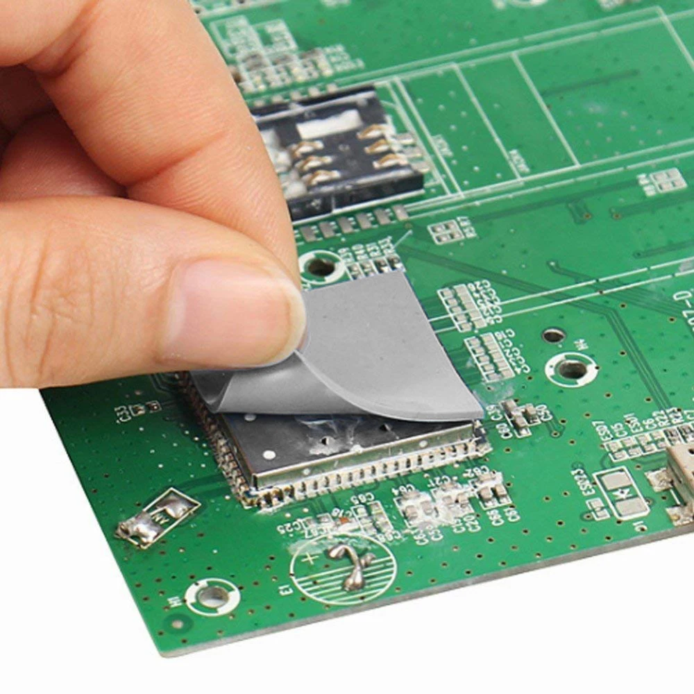
- Place Thermal Pads Directly Under Heat-Generating Components: Components like power transistors, voltage regulators, and LEDs generate significant heat. Positioning thermal pads directly beneath these components ensures efficient heat transfer to the PCB substrate or heat sink. For example, a MOSFET dissipating 3W of heat should have a thermal pad area of at least 1.5 times the component’s footprint for adequate dissipation.
- Ensure Adequate Pad Size: The size of the thermal pad should match the heat dissipation needs of the component. A general rule of thumb is to make the pad area at least 1.2 to 1.5 times larger than the component’s base to handle thermal loads effectively.
- Avoid Overlapping with Other Pads: Overlapping thermal pads with other conductive areas can lead to unintended short circuits or uneven heat distribution. Maintain a clearance of at least 0.5mm between thermal pads and nearby traces or pads.
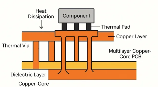
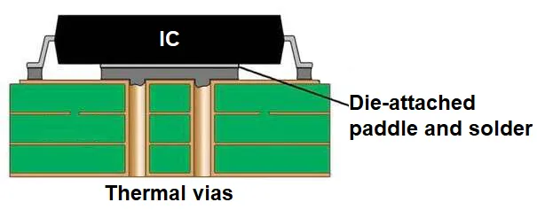
- Consider Board Layer Stackup: In multi-layer PCBs, thermal pads on inner layers can help distribute heat across the board. Ensure vias are used to connect these pads to surface layers or ground planes for better heat sinking.
By adhering to these placement rules, you can prevent hotspots and ensure that heat is managed effectively across the board.
Thermal Pad Proximity to Components: Striking the Right Balance
The thermal pad proximity to components plays a crucial role in both heat dissipation and overall board reliability. While placing thermal pads close to heat-generating components is necessary, getting too close to sensitive parts can introduce unwanted thermal stress. Here are some key considerations:
- Close Proximity for Heat Sources: For high-power components, thermal pads should be as close as possible—ideally directly beneath the component. This minimizes thermal resistance and allows heat to transfer quickly to the pad. For instance, a 2W LED should have a thermal pad within 0.2mm of its base for optimal performance.
- Distance from Sensitive Components: Components like microcontrollers or sensors can be sensitive to heat. Maintain a distance of at least 3mm between thermal pads and such components to prevent thermal interference. If space is limited, consider adding thermal barriers or smaller heat sinks.
- Balancing Heat Distribution: If multiple components are generating heat in close proximity, distribute thermal pads evenly to avoid creating localized hotspots. This ensures that no single area of the PCB is overwhelmed by thermal load.
Striking the right balance in proximity helps protect sensitive components while ensuring effective heat management for high-power elements.
Effective Thermal Relief Pad Design for Soldering and Heat Management
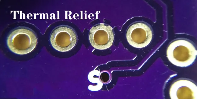
A well-thought-out thermal relief pad design is vital for both manufacturability and thermal performance. Thermal relief pads are modified pad designs that reduce heat sinking during soldering, making it easier to achieve strong solder joints while still providing heat dissipation during operation. Here’s how to design them effectively:
- Use Spoke Patterns: Thermal relief pads typically feature a spoke-like pattern connecting the pad to the surrounding copper plane. A common design includes four spokes, each with a width of 0.3mm to 0.5mm, to balance heat transfer and soldering ease. This design reduces the amount of heat pulled away during soldering, ensuring a reliable joint.
- Optimize Spoke Length and Thickness: The length and thickness of the spokes should be tailored to the component’s heat dissipation needs. For a component dissipating 1W, spokes of 0.8mm in length can provide adequate thermal isolation during soldering while still allowing heat transfer during operation.
- Match Pad Size to Component: Ensure the thermal relief pad matches the footprint of the component. Oversized pads can lead to excessive heat sinking, while undersized pads may not provide enough thermal relief.
Proper thermal relief pad design prevents soldering defects like cold joints while maintaining effective heat dissipation during normal operation. This dual benefit is critical for long-term PCB reliability.
Thermal Pad Connection to Ground Plane: Enhancing Heat Dissipation
The thermal pad connection to ground plane is a powerful technique for improving heat dissipation across the entire PCB. Ground planes act as large heat sinks, spreading thermal energy over a wide area and reducing localized temperature spikes. Here’s how to make the most of this connection:
- Direct Connection for Maximum Heat Transfer: Connect thermal pads directly to the ground plane using multiple vias. For a thermal pad under a 5W power component, use at least 4 to 6 vias with a diameter of 0.3mm each to ensure efficient heat transfer. This can reduce local temperatures by up to 20°C in high-power applications.
- Use Thermal Vias Strategically: Place thermal vias in a grid pattern beneath the pad to maximize heat flow to the ground plane. Space vias approximately 1mm apart to avoid weakening the board structure while still achieving effective heat distribution.
- Consider Ground Plane Size: The effectiveness of heat dissipation depends on the size of the ground plane. A larger ground plane (covering 50% or more of the board area) can handle higher thermal loads, while smaller planes may require additional heat sinks or cooling solutions.
Connecting thermal pads to the ground plane is a simple yet effective way to manage heat across the board, especially in compact designs with limited space for external cooling.
Thermal Pad Influence on Component Lifespan
The thermal pad influence on component lifespan cannot be overstated. Excessive heat is one of the leading causes of component failure, and thermal pads play a direct role in mitigating this risk. Here’s how proper thermal pad design and placement impact longevity:
- Reducing Operating Temperatures: Components operating at high temperatures (above 85°C for extended periods) can experience a 50% reduction in lifespan. Effective thermal pads can lower operating temperatures by 10-20°C, doubling the expected lifespan of components like power ICs or LEDs.
- Preventing Thermal Cycling Stress: Repeated heating and cooling cycles can cause mechanical stress on solder joints and component leads, leading to cracks or failures. Well-placed thermal pads minimize temperature fluctuations, reducing thermal cycling stress by up to 30% in high-power designs.
- Protecting Sensitive Components: By directing heat away from sensitive areas, thermal pads help maintain stable conditions for components like microcontrollers, which can fail if exposed to temperatures above 105°C for prolonged periods.
Investing time in strategic thermal pad placement and design directly translates to longer-lasting, more reliable PCBs. This not only reduces maintenance costs but also enhances the overall performance of your electronic devices.
Best Practices for Implementing Thermal Pads in Your PCB Design
To wrap up, let’s summarize some best practices for integrating thermal pads into your PCB designs. These actionable tips will help you maximize reliability and performance:
- Simulate Thermal Performance: Use PCB design software with thermal simulation tools to predict heat distribution and identify potential hotspots before manufacturing. Aim for a maximum temperature rise of no more than 20°C above ambient under full load.
- Collaborate with Manufacturers: Work closely with your PCB fabrication team to ensure thermal pad designs meet manufacturing capabilities, especially for complex multi-layer boards with thermal vias.
- Test Under Real Conditions: After prototyping, test your PCB under realistic operating conditions to verify thermal performance. Use infrared cameras to detect hotspots and adjust pad placement or size as needed.
- Stay Updated on Materials: Choose PCB substrates with high thermal conductivity (e.g., materials with a thermal conductivity of 1.0 W/mK or higher) to complement thermal pad performance.
By following these practices, you can ensure that your thermal pad strategy aligns with both design goals and real-world performance needs.
Conclusion: Elevate Your PCB Design with Strategic Thermal Pad Placement
Thermal management is a cornerstone of reliable PCB design, and strategic thermal pad placement is at the heart of this process. By adhering to PCB thermal pad placement rules, optimizing thermal pad proximity to components, focusing on effective thermal relief pad design, leveraging thermal pad connection to ground plane, and understanding the thermal pad influence on component lifespan, you can create boards that perform consistently and last longer.
Implementing these strategies doesn’t just prevent failures—it enhances the overall quality of your electronic products. Take the time to plan and simulate your thermal pad layout, and you’ll see the difference in both performance and reliability. With the right approach, your PCB designs can withstand the heat and keep delivering results.