 ALLPCB


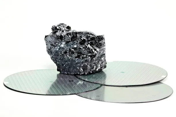
The main techniques for growing SiC crystals are physical vapor transport, high-temperature solution growth, and high-temperature chemical vapor deposition.
Interest in SiC materials has increased in recent years as the technology has progressed. Years before broader attention, some developers recognized SiC's advantages and began applying it in high-performance applications. In one example, a racing team replaced an IGBT+Si FRD solution with an IGBT+SiC SBD solution, which reduced vehicle mass by about 2 kg and reduced component size by 19%. The following year, the vehicle's power module was further upgraded to SiC MOS devices, which reduced mass by an additional 6 kg and further reduced size by about 43%. The high-voltage control level was increased from 200 kV to 220 kV. The successful application of SiC power devices contributed to wider industry attention and to SiC devices being adopted beyond specialist racing applications.
Physical Vapor Transport (PVT)
The first method is physical vapor transport, commonly abbreviated PVT. This method is analogous to steaming: SiC powder is heated until it vaporizes, and the vapor cools and crystallizes at a lower temperature region. In PVT growth, SiC powder is placed at the bottom of a furnace and heated. At temperatures around 2000–2500°C the powder decomposes into gaseous species. Relevant reaction pathways include:
- SiC(s) = Si(g) + C(s)
- 2SiC(s) = Si(g) + SiC2(g)
- 2SiC(s) = C(s) + Si2C(g)
During SiC crystallization, reactions such as the following can occur:
- Si2C(g) + SiC2(g) = 3SiC(s)
- Si(g) + SiC2(g) = 2SiC(s)
Because the furnace bottom is hotter than the top, vapor condenses at the cooler upper region and grows along the seed crystal direction, ultimately forming an SiC crystal.
PVT equipment is relatively simple to build and operate, making PVT the current mainstream method for SiC crystal growth. However, PVT has drawbacks: it is relatively difficult to enlarge wafer diameter—for example, expanding a 4-inch boule to 6-inch or 8-inch diameters requires long growth cycles—and it offers limited advantages for dopant incorporation control.
High-Temperature Solution Growth
The second method is high-temperature solution growth, which uses a solvent to dissolve carbon and transport it to the growth front.
Solubility generally depends on temperature. For example, dissolved sugar can precipitate as a solution cools because solubility decreases with temperature. In high-temperature solution growth for SiC, a metal solvent such as chromium is used. Although chromium is solid at room temperature, at high temperature it melts and functions as a liquid solution.
SiC and Cr are placed in a graphite crucible. The molten Cr acts as a transport medium, carrying carbon from the lower region of the furnace to the upper region, where cooling and crystallization on a seed produce SiC crystal growth.
Advantages of high-temperature solution growth include low dislocation density, which addresses a key limitation for SiC device performance; relative ease of diameter enlargement; and the ability to obtain p-type crystals.
Limitations include solvent sublimation at high temperature, impurity concentration control in the grown crystal, solvent inclusions, and formation of floating crystals.
High-Temperature Chemical Vapor Deposition (HTCVD)
The third method is high-temperature chemical vapor deposition (HTCVD). Unlike the previous two methods, which use SiC powder as the source, HTCVD uses gaseous organic precursors that contain silicon and carbon.
In HTCVD, gases are introduced into a furnace through piping, and chemical reactions in the furnace deposit SiC crystals.
HTCVD is still in the research stage for SiC bulk crystal growth. The technique requires complex equipment and currently has high costs, so it is not yet a mainstream growth method.


