If you're stepping into the world of high-speed digital PCB design as a beginner, you might be wondering where to start. High-speed design is crucial for modern electronics, ensuring signals travel quickly and reliably in devices like smartphones, computers, and IoT gadgets. This guide offers a clear starting point, covering the basics of high-speed design, PCB materials, simulation tools, and even open-source software options to help you learn PCB design effectively. Let’s dive into this detailed introduction to build a strong foundation for your projects.
What Is High-Speed Digital PCB Design?
High-speed digital PCB design refers to creating printed circuit boards that handle fast signal transitions, typically above 50 MHz, where signal integrity becomes critical. Unlike low-speed designs, high-speed circuits require careful attention to trace layout, impedance control, and noise reduction to prevent issues like signal distortion or data loss. Think of it as designing a highway for data—any bumps or sharp turns can slow down or crash the information flow.
In this field, engineers focus on minimizing delays and ensuring signals arrive at their destination without interference. For beginners, understanding the core principles of high-speed design is the first step to mastering complex electronics projects. This blog will break down those principles into manageable pieces, helping you learn PCB design for high-speed applications.
Why High-Speed Design Matters in Modern Electronics
Modern devices rely on high-speed PCBs to process data quickly. For example, a typical USB 3.0 interface operates at 5 Gbps, requiring precise design to avoid signal degradation over short distances. Without proper high-speed design, you might face issues like crosstalk (unwanted signal interference) or electromagnetic interference (EMI), which can disrupt device performance.
For beginners, the stakes are high because a small mistake in layout or material choice can lead to costly redesigns. By learning the basics of high-speed design, you can avoid common pitfalls and create reliable boards for applications like high-frequency communication or fast data processing.
Key Challenges in High-Speed Digital PCB Design
High-speed design introduces unique challenges that beginners must understand. Here are the main hurdles:
- Signal Integrity: Fast signals can distort due to reflections or mismatched impedance. For instance, a signal traveling at 1 GHz can reflect back if the trace impedance isn’t controlled to 50 ohms, a common standard for high-speed lines.
- Crosstalk: Nearby traces can interfere with each other, especially if they’re too close. Spacing traces at least 3 times the trace width apart can reduce this risk.
- Power Integrity: High-speed circuits need stable power delivery. A poorly placed decoupling capacitor can cause voltage drops, affecting performance.
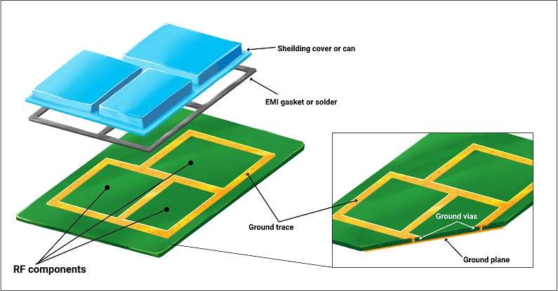
- EMI: Fast-switching signals can emit electromagnetic noise, interfering with other components or violating regulatory standards.
Addressing these challenges requires a mix of good design practices, the right tools, and suitable materials. Let’s explore these elements in detail.
Understanding PCB Materials for High-Speed Design
Choosing the right PCB materials is critical for high-speed design. The material affects how signals propagate through the board and how much loss or interference occurs. For beginners looking to learn PCB design, here’s a breakdown of key material properties and options:
Dielectric Constant (Dk) and Loss Tangent (Df)
The dielectric constant determines how much a material slows down a signal, while the loss tangent measures signal energy loss as heat. For high-speed designs, you want a material with a low Dk (around 3.5 or less) and a low Df (below 0.005) to minimize delays and losses. For comparison, standard FR-4 material has a Dk of about 4.5, which may not be ideal for frequencies above 1 GHz.
Common Materials for High-Speed PCBs
- FR-4: A cost-effective option for lower-speed designs (up to 500 MHz). It’s widely used but not ideal for very high frequencies due to higher signal loss.
- High-Speed Laminates: Materials like Isola IS620 or Rogers RO4350B offer lower Dk and Df values, making them suitable for multi-GHz applications. They’re more expensive but necessary for advanced projects.
- PTFE-Based Materials: These provide excellent performance at high frequencies (above 5 GHz) but are costly and harder to work with for beginners.
For most beginner projects, starting with FR-4 is fine, but as you tackle faster designs, consider upgrading to high-speed laminates. Always check the material’s specifications to match your signal speed requirements.
Core Principles of High-Speed PCB Layout
A well-designed layout is the backbone of high-speed digital PCB design. Here are essential tips to follow as you learn PCB layout techniques:
Impedance Matching
High-speed signals require consistent impedance along their path to prevent reflections. For example, a 50-ohm impedance is standard for many high-speed interfaces like USB or Ethernet. Use trace width calculators to ensure your traces match the target impedance based on your board’s material and stack-up.
Trace Length and Routing
Keep high-speed traces as short and direct as possible to minimize delays. If traces must be longer, match their lengths in differential pairs (like USB data lines) to within 5 mils (0.005 inches) to avoid timing skew. Avoid sharp 90-degree bends; use 45-degree angles or curves to reduce signal reflections.
Ground Planes
A solid ground plane under high-speed traces reduces noise and provides a return path for signals. Avoid splitting the ground plane under critical traces, as this can disrupt signal integrity.
Component Placement
Place components to minimize trace lengths for high-speed signals. For instance, position decoupling capacitors within 0.1 inches of a chip’s power pins to filter noise effectively.
By following these guidelines, beginners can create layouts that support high-speed performance while avoiding common errors.
The Role of PCB Simulation in High-Speed Design
PCB simulation is a powerful tool for predicting how your design will perform before manufacturing. For high-speed projects, simulation helps identify signal integrity issues, EMI risks, and power delivery problems early in the process.
Types of Simulations
- Signal Integrity Simulation: Analyzes how signals behave over traces, checking for reflections or crosstalk. Tools can simulate a 2.5 GHz signal to ensure it meets timing requirements.
- Power Integrity Simulation: Ensures stable voltage across the board, identifying areas where decoupling capacitors are needed.
- EMI Simulation: Predicts electromagnetic interference, helping you adjust layouts to meet regulatory standards.
Benefits for Beginners
Simulation saves time and money by catching errors before you build a prototype. For instance, discovering a mismatched impedance through simulation is far cheaper than fixing a batch of faulty boards. Many design tools now include basic simulation features, making them accessible even if you’re just starting to learn PCB design.
Exploring Open-Source PCB Software for High-Speed Design
For beginners, cost can be a barrier to learning PCB design. Open-source PCB software offers a free or low-cost way to practice high-speed design without sacrificing essential features. Here are some popular options worth exploring:
- KiCad: A robust open-source tool with schematic capture and PCB layout capabilities. It supports high-speed design through plugins for impedance calculation and signal integrity checks.
- Fritzing: Ideal for absolute beginners, though limited for complex high-speed projects. It’s great for learning basic concepts before moving to advanced tools.
- FreeCAD (with PCB extensions): While primarily a 3D modeling tool, extensions allow basic PCB design, though it’s not optimized for high-speed applications.
These tools often have active communities where you can find tutorials and support. While they may lack some advanced simulation features of premium software, they’re a fantastic starting point for high-speed design practice.
Step-by-Step Guide to Starting Your First High-Speed PCB Project
Ready to apply what you’ve learned? Follow these steps to design your first high-speed PCB:
- Define Your Requirements: Determine the signal speed (e.g., 100 MHz or 1 GHz) and interface standards (like USB 2.0) your project needs.
- Choose Materials: Select a PCB material based on frequency. Use FR-4 for lower speeds or a high-speed laminate for faster signals.
- Create a Schematic: Draw your circuit using open-source software, ensuring all high-speed components are accounted for.
- Design the Layout: Follow impedance matching and routing guidelines. Keep high-speed traces short and use ground planes.
- Simulate Your Design: Use built-in or external tools to check signal integrity and power delivery.
- Review and Iterate: Double-check your design rules and make adjustments based on simulation results.
- Manufacture and Test: Once satisfied, send your design for fabrication and test the board with real signals.
This process gives beginners a clear path to learn PCB design while tackling the challenges of high-speed projects.
Tips for Success in High-Speed PCB Design
As you build your skills, keep these tips in mind:
- Start with simple projects (e.g., a basic USB interface) before moving to complex designs like DDR memory layouts.
- Study datasheets for high-speed components to understand their layout recommendations.
- Join online forums or communities to learn from experienced designers and share your progress.
- Invest time in learning simulation tools, as they’re invaluable for catching errors early.
Common Mistakes to Avoid as a Beginner
High-speed design can be tricky, and beginners often make these mistakes:
- Ignoring impedance control, leading to signal reflections.
- Routing high-speed traces over split ground planes, causing noise issues.
- Using inappropriate materials for the signal frequency, resulting in excessive loss.
- Skipping simulation, which can miss critical flaws until testing.
By being aware of these pitfalls, you can save time and create more reliable designs from the start.
Conclusion: Your Journey to Mastering High-Speed PCB Design
High-speed digital PCB design may seem daunting at first, but with the right knowledge and tools, beginners can build a strong foundation. From understanding PCB materials and mastering layout techniques to using PCB simulation and open-source software, every step you take brings you closer to creating reliable, high-performance boards. Start small, practice consistently, and leverage the resources available to learn PCB design effectively.
At ALLPCB, we’re committed to supporting your journey with resources and services tailored to your needs. Whether you’re experimenting with your first high-speed project or scaling up to complex designs, the principles covered in this guide will help you succeed. Keep learning, designing, and pushing the boundaries of what’s possible in electronics.
 ALLPCB


