ALLPCB


If you're diving into the world of printed circuit boards (PCBs), understanding copper weight variations is crucial for ensuring your design performs as expected. Copper weight, often tied to thickness, directly impacts current capacity, heat dissipation, and signal integrity. Variations in copper weight during manufacturing can affect your PCB's reliability, so knowing about PCB copper thickness tolerance, copper weight manufacturing variations, and controlling copper thickness in PCB production is essential. In this blog, we'll break down these concepts, explore why they matter, and provide actionable insights to help you navigate these challenges in PCB manufacturing.
What Is Copper Weight in PCB Manufacturing?
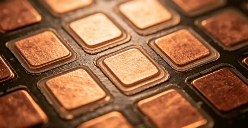
Copper weight refers to the amount of copper used on a PCB layer, typically measured in ounces per square foot (oz/ft2). This measurement correlates to the thickness of the copper layer. For instance, 1 oz/ft2 of copper translates to a thickness of about 1.37 mils (0.00137 inches or 34.8 micrometers). Common copper weights in PCB manufacturing range from 0.5 oz/ft2 to 3 oz/ft2 or higher for heavy-duty applications.
Why does this matter? The copper weight determines how much current a trace can carry without overheating and how well it can manage thermal dissipation. A mismatch or variation in copper weight can lead to performance issues, such as signal loss or board failure under high current loads. Understanding and controlling copper weight variations ensures your PCB meets design specifications and performs reliably.
Why Do Copper Weight Variations Occur in PCB Manufacturing?
During PCB production, several factors contribute to copper weight manufacturing variations. These variations can stem from the raw materials, the manufacturing process, or even design choices. Let's explore the primary causes:
- Base Material Tolerances: The copper foil used in PCBs often has inherent thickness variations from the supplier. Even high-quality foils can vary slightly, impacting the final copper weight on the board.
- Plating Process: Copper plating, used to build up thickness on traces and vias, isn't always uniform. Factors like current density in the plating bath can lead to uneven deposition, creating thicker or thinner areas on the board.
- Copper Balance: If a PCB design has uneven copper distribution (e.g., dense traces on one side and sparse on the other), it can cause variations during etching and plating, as the processes may not apply evenly across the board.
- Etching Variations: The etching process, which removes unwanted copper, can sometimes over-etch or under-etch, leading to inconsistent thicknesses across the board.
- Galvanic Effects: During plating, galvanic effects can cause more copper to deposit in certain areas, especially near edges or high-current zones, leading to uneven thickness.
These factors highlight the complexity of achieving uniform copper weight and why PCB copper thickness tolerance is a critical specification in manufacturing standards.
Understanding PCB Copper Thickness Tolerance
PCB copper thickness tolerance refers to the acceptable range of variation in copper thickness (or weight) on a PCB as defined by industry standards. The most widely recognized standard comes from the IPC (Institute of Printed Circuits), specifically IPC-6012, which categorizes PCBs into different classes based on their application and reliability requirements.
For instance:
- Class 2 PCBs (general electronic products): For a specified copper weight of 1 oz/ft2, the tolerance might allow a range of 0.8 to 1.2 oz/ft2, equivalent to a thickness of approximately 28 to 42 micrometers.
- Class 3 PCBs (high-reliability products, such as aerospace or medical devices): The tolerance is tighter, often ranging from 0.9 to 1.1 oz/ft2, or about 31.5 to 38.5 micrometers for the same 1 oz/ft2 specification.
These tolerances are in place to ensure that even with manufacturing variations, the PCB can still meet performance expectations. However, exceeding these tolerances can lead to issues like reduced current-carrying capacity or impedance mismatches, especially in high-frequency designs where signal integrity is critical.
Impacts of Copper Weight Variations on PCB Performance
Copper weight variations aren't just a manufacturing concern—they directly affect how a PCB performs in real-world applications. Here's how these variations can impact your design:
- Current-Carrying Capacity: Thinner copper layers carry less current. For example, a trace with 1 oz/ft2 copper can safely handle about 1-2 amps depending on width, but if the thickness drops to 0.8 oz/ft2 due to variation, the capacity decreases, risking overheating and potential failure.
- Thermal Management: Copper dissipates heat generated by components. Uneven or thinner copper can lead to hot spots, reducing the lifespan of the board and components.
- Signal Integrity and Impedance Control: In high-speed designs, copper thickness affects impedance. A variation of even 10% in thickness can shift impedance values outside acceptable ranges (e.g., from 50 ohms to 55 ohms), causing signal reflections and data errors.
- Mechanical Strength: Thicker copper provides better mechanical stability, especially in multilayer boards. Variations can lead to weak spots prone to cracking under stress.
These effects underscore the importance of controlling copper thickness in PCB manufacturing to ensure consistent performance across all boards in a production run.
Strategies for Controlling Copper Thickness in PCB Manufacturing
While some variation is inevitable, there are several strategies for controlling copper thickness in PCB production to minimize deviations and ensure reliability. Here are practical steps for designers and manufacturers:
1. Choose the Right Copper Weight for Your Application
Select a copper weight that matches your design's requirements for current, thermal management, and signal integrity. For low-power applications, 0.5 or 1 oz/ft2 may suffice, while high-power designs might need 2 or 3 oz/ft2. Keep in mind that thicker copper often comes with tighter tolerances but increases cost.
2. Design for Uniform Copper Distribution
Avoid large disparities in copper density across the board. Use dummy fills or balance copper areas in your layout to ensure even plating and etching. This reduces the risk of uneven thickness caused by galvanic effects or over-etching in sparse areas.
3. Specify Tight Tolerances in Your Design Files
Clearly define the acceptable PCB copper thickness tolerance in your design specifications. Reference IPC standards (like IPC-6012) to ensure the manufacturer understands the required class and tolerance levels for your project.
4. Partner with a Reliable Manufacturer
Work with a manufacturer that has advanced process controls for plating and etching. Discuss their capabilities early in the design phase to understand their limits on copper thickness variations. Some manufacturers use higher-quality copper foils or automated plating systems to achieve better consistency.
5. Use Consistent Copper Thickness Across Layers
Maintain the same copper weight across all layers of a multilayer PCB whenever possible. Sudden changes in thickness between layers can create manufacturing challenges and lead to impedance mismatches or reliability issues.
6. Incorporate Testing and Inspection
Request post-production testing, such as cross-sectional analysis or electrical testing, to verify copper thickness. Non-destructive methods like X-ray fluorescence (XRF) can measure copper weight without damaging the board, ensuring it meets your specified tolerances.
Common Copper Weights and Their Applications
Choosing the right copper weight is a balancing act between performance, cost, and manufacturability. Here's a quick guide to common copper weights and their typical uses:
- 0.5 oz/ft2 (17.5 μm): Used in low-power, high-density designs where space and weight are critical, such as in mobile devices. Offers limited current capacity.
- 1 oz/ft2 (34.8 μm): The industry standard for most general-purpose PCBs. Suitable for moderate current and signal applications, balancing cost and performance.
- 2 oz/ft2 (69.6 μm): Common in power electronics where higher current and better heat dissipation are needed, such as in motor controllers or power supplies.
- 3 oz/ft2 and above (104.4 μm+): Used in heavy copper PCBs for high-power applications like industrial equipment or automotive systems. Provides excellent thermal management but increases cost and manufacturing complexity.
Understanding these options helps you make informed decisions while considering potential copper weight manufacturing variations during production.
Conclusion: Mastering Copper Weight for Better PCB Designs
Copper weight variations are an inevitable part of PCB manufacturing, but with the right knowledge and strategies, you can minimize their impact on your designs. By understanding PCB copper thickness tolerance, recognizing the causes of copper weight manufacturing variations, and implementing techniques for controlling copper thickness in PCB production, you can ensure your boards meet performance and reliability standards.
Start by selecting the appropriate copper weight for your application, designing for uniform copper distribution, and specifying clear tolerances. Partnering with a capable manufacturer and incorporating testing further reduces risks. With these steps, you'll be well-equipped to handle copper weight variations and create PCBs that perform consistently, whether for consumer electronics, industrial systems, or high-reliability applications.
At ALLPCB, we're committed to helping you achieve precision and quality in every board. By focusing on tight process controls and clear communication, we aim to deliver PCBs that meet your exact specifications, minimizing variations and maximizing performance.