ALLPCB


In the world of power electronics, designing a printed circuit board (PCB) that can handle high current, manage thermal challenges, and minimize voltage drop is critical. The outer layer of a PCB plays a significant role in achieving these goals, as it directly impacts heat dissipation, current carrying capacity, and overall performance. For engineers working on power electronics applications, optimizing the outer layer PCB design is a key step in ensuring reliability and efficiency.
In this comprehensive guide, we’ll dive deep into the essentials of outer layer PCB design for power electronics. We’ll cover thermal management strategies, high current handling, voltage drop reduction, and effective PCB layout techniques. Whether you’re designing for industrial power supplies, electric vehicle systems, or renewable energy converters, this blog will provide actionable insights to enhance your designs with a focus on power electronics, thermal management, high current, voltage drop, and PCB layout.
Why Outer Layer PCB Design Matters in Power Electronics
Power electronics applications often involve high power levels, which translate to significant current and voltage demands on a PCB. The outer layers of a PCB are crucial because they are directly exposed to the environment, making them primary paths for heat dissipation and current flow. A well-designed outer layer can prevent overheating, reduce electrical losses, and improve the lifespan of components.
In power electronics, the outer layer often hosts critical traces for high current paths, heat sinks, and mounting points for power components like MOSFETs and IGBTs. Poor design in this area can lead to thermal hotspots, increased voltage drop, and even board failure. By focusing on the outer layer during the PCB layout process, you can address these challenges early and create a more robust system.
Key Considerations for Outer Layer PCB Design in Power Electronics
Designing the outer layer of a PCB for power electronics requires careful attention to several factors. Below, we break down the most important considerations to guide your design process.
1. Thermal Management for Heat Dissipation
Thermal management is one of the biggest challenges in power electronics. Components like power transistors and diodes generate significant heat during operation, and if this heat isn’t managed properly, it can degrade performance or cause failure. The outer layer of a PCB is your first line of defense against overheating.
To improve thermal performance, consider using wider copper traces on the outer layer to act as heat spreaders. Copper has excellent thermal conductivity, and increasing the surface area of traces helps dissipate heat more effectively. Additionally, place thermal vias near high-power components to transfer heat from the outer layer to inner layers or a heat sink. For instance, a typical design might use vias with a diameter of 0.3 mm spaced 1 mm apart to achieve a thermal resistance of less than 10°C/W.
Another strategy is to use thicker copper layers on the outer surface. Standard PCBs often use 1 oz/ft2 copper (about 35 μm thick), but for power electronics, opting for 2 oz/ft2 or even 3 oz/ft2 copper can significantly improve heat dissipation and current handling.
2. Handling High Current with Proper Trace Widths
High current is a defining feature of power electronics, and the outer layer often carries the bulk of this current through wide traces. If the traces are too narrow, they can overheat due to high current density, leading to increased resistance and potential board damage.
To handle high current, calculate the appropriate trace width based on the expected current and acceptable temperature rise. A common guideline is to use a trace width calculator to ensure the current density stays below 5 A/mm2 for a 10°C temperature rise. For example, a 10 A current might require a trace width of 2 mm on a 1 oz/ft2 copper layer. Wider traces or thicker copper can reduce resistance further, minimizing heat generation.
Additionally, consider placing high current traces on the outer layer to take advantage of better airflow for cooling. Avoid routing sensitive signal traces near these paths to prevent electromagnetic interference (EMI), which is a common issue in power electronics designs.
3. Minimizing Voltage Drop Across Traces
Voltage drop is a critical concern in power electronics, especially when dealing with high current over long traces. Voltage drop occurs due to the resistance of the copper traces, and even a small drop can affect the performance of power components, leading to inefficiencies.
To minimize voltage drop, keep high current traces as short and wide as possible on the outer layer. The resistance of a trace is directly proportional to its length and inversely proportional to its width and thickness. For instance, a 100 mm long trace with a width of 1 mm on a 1 oz/ft2 copper layer might have a resistance of about 0.05 ohms, leading to a 0.5 V drop at 10 A. Doubling the width to 2 mm reduces the resistance to 0.025 ohms, cutting the voltage drop in half.
Using multiple parallel traces or adding copper pours on the outer layer can further reduce resistance and distribute current more evenly. This approach is especially useful for power supply lines in high current applications.
4. Optimizing PCB Layout for Power Electronics
The overall PCB layout plays a vital role in the performance of the outer layer. A well-thought-out layout ensures efficient current flow, reduces EMI, and enhances thermal management. Here are some key tips for optimizing your PCB layout:
- Separate Power and Signal Layers: Place high current power traces on the outer layer and sensitive signal traces on inner layers to minimize interference. This separation helps maintain signal integrity in power electronics systems.
- Use Ground Planes: A solid ground plane on the outer or inner layer can reduce noise and provide a low-impedance return path for currents, which is essential for high current designs.
- Position Components Strategically: Place high-power components near the edges of the board on the outer layer to allow better access to heat sinks or airflow. Keep decoupling capacitors close to power pins to stabilize voltage.
- Route with Short Paths: Minimize the length of high current traces by routing them directly between components on the outer layer. Long traces increase resistance and voltage drop.
By following these layout practices, you can create a PCB design that balances thermal management, high current handling, and voltage drop reduction effectively.
Material Selection for Outer Layer PCB Design
The choice of materials for your PCB can significantly impact the performance of the outer layer in power electronics applications. Standard FR-4 material is common for many designs, but it may not always be the best choice for high-power systems due to its limited thermal conductivity (approximately 0.3 W/m·K).
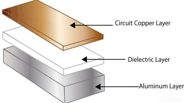
For better thermal management, consider using high thermal conductivity substrates like metal-core PCBs (MCPCBs) or ceramics. Aluminum-based MCPCBs, for example, offer thermal conductivity values of 1-2 W/m·K, making them ideal for dissipating heat from the outer layer. These materials are particularly useful in applications like LED drivers or motor controllers, where heat generation is a constant concern.
Additionally, opt for higher copper weights on the outer layer, as mentioned earlier. Thicker copper not only improves current carrying capacity but also aids in spreading heat more evenly across the board.
Advanced Techniques for Outer Layer Design
For engineers looking to push the boundaries of power electronics design, advanced techniques can further enhance outer layer performance. One such method is the use of embedded heat sinks or copper coins directly under high-power components on the outer layer. These inserts provide a direct thermal path to dissipate heat, reducing the thermal resistance to as low as 5°C/W in some designs.
Another technique is to implement selective copper plating on the outer layer. This process allows you to increase copper thickness only in high current areas, optimizing both cost and performance. For instance, a selective plating of 4 oz/ft2 copper in power trace areas can handle currents up to 20 A without excessive heating.
Finally, consider using simulation tools to model thermal and electrical performance before fabrication. Software can predict hotspots, voltage drops, and current density issues on the outer layer, allowing you to refine your design early in the process.
Common Challenges and Solutions in Outer Layer PCB Design
Designing the outer layer for power electronics isn’t without its challenges. Here are some common issues and how to address them:
- Thermal Hotspots: Use thermal vias, wider traces, and heat sinks to spread heat evenly. Simulation tools can help identify problem areas before manufacturing.
- High Voltage Drop: Shorten trace lengths, increase trace width, and use thicker copper to reduce resistance. Parallel traces or copper pours can also help.
- EMI Issues: Keep high current traces on the outer layer away from sensitive signals. Use ground planes to shield against interference.
By anticipating these challenges during the design phase, you can create a more reliable and efficient PCB for power electronics applications.
Conclusion: Building Better Power Electronics with Outer Layer PCB Design
Outer layer PCB design is a cornerstone of successful power electronics applications. By focusing on thermal management, high current handling, voltage drop reduction, and optimized PCB layout, you can create boards that perform reliably under demanding conditions. From selecting the right materials to implementing advanced techniques like embedded heat sinks, every decision in the design process impacts the final outcome.
At ALLPCB, we understand the unique needs of power electronics engineers. Our expertise in PCB manufacturing ensures that your designs are brought to life with precision and quality, helping you achieve optimal performance in thermal management and high current applications. Start refining your outer layer PCB design today to power up your next project with confidence.