 ALLPCB


Introduction
High-density interconnect (HDI) printed circuit boards represent a critical advancement in electronics, enabling compact designs with superior performance for applications in telecommunications, medical devices, and aerospace. Compliance with established standards ensures these boards meet rigorous quality, reliability, and environmental requirements throughout their lifecycle. For electrical engineers working on complex systems, understanding HDI PCB IPC standards is essential to avoid costly redesigns and production delays. This article explores key IPC standards like IPC-2226 and IPC-6012, alongside regulatory frameworks such as RoHS compliance and REACH compliance. By aligning designs and manufacturing processes with these guidelines, engineers can achieve optimal functionality and market readiness. Factory-driven insights reveal that proactive compliance integration from the design phase minimizes defects and enhances long-term board integrity.
Understanding HDI PCBs and the Need for Compliance
HDI PCBs feature finer lines, smaller vias, and advanced layering techniques compared to conventional boards, packing more interconnects into smaller footprints. This density demands precise adherence to industry benchmarks to prevent issues like signal integrity loss or mechanical failure. HDI PCB IPC standards provide the foundational rules for design and fabrication, ensuring consistency across supply chains. Without compliance, boards risk failing qualification tests or exhibiting premature wear under thermal or mechanical stress. Electrical engineers must prioritize these standards to support high-reliability applications where downtime is unacceptable. Ultimately, compliance bridges the gap between innovative design and manufacturable reality, fostering trust in the final product.
Key IPC Standards for HDI PCB Design and Performance
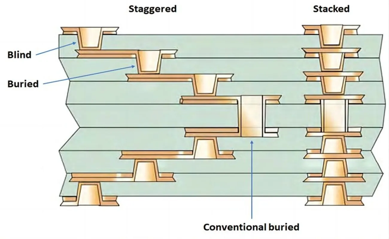
IPC-2226 serves as the sectional design standard specifically for high-density interconnect printed boards, outlining requirements for microvia configurations, layer stackups, and fine-pitch features. It classifies HDI structures into types based on via types, such as blind, buried, or stacked microvias, guiding engineers in selecting appropriate build-ups for their application's routing density. This standard emphasizes considerations for material selection, via formation, and interconnect reliability to accommodate the challenges of sequential lamination processes. Complementing design efforts, IPC-6012 defines qualification and performance specifications for rigid printed boards, including those with HDI features. It establishes criteria for electrical, mechanical, and environmental testing across performance classes, from general consumer to high-reliability aerospace grades. Together, these HDI PCB IPC standards form a cohesive framework that factory processes must validate through rigorous inspection and testing protocols.
Engineers should note that IPC-2226 integrates with broader generic design guidelines, providing tailored rules for HDI's unique aspects like aspect ratios and plating thicknesses. Compliance involves verifying trace widths, spacing, and via capture pads against these parameters during layout reviews. IPC-6012 then shifts focus to post-fabrication verification, specifying bow and twist limits, solderability, and continuity resistance to ensure the board performs as designed. Factory insights highlight that deviations in microvia reliability often stem from non-compliance here, leading to opens or shorts in high-volume production. By embedding these standards into design rules and process controls, teams reduce variability and accelerate time-to-market.
Navigating RoHS and REACH Compliance in HDI Manufacturing
RoHS compliance restricts hazardous substances like lead, mercury, cadmium, hexavalent chromium, polybrominated biphenyls, and polybrominated diphenyl ethers in electrical and electronic equipment. For HDI PCBs, this translates to selecting lead-free surface finishes such as immersion tin or electroless nickel immersion gold, alongside halogen-free laminates to support higher soldering temperatures. Electrical engineers must audit material declarations from suppliers to confirm concentrations stay below 0.1% by weight, as non-compliant finishes can compromise solder joint integrity in dense interconnects. Factories implement segregated process lines for RoHS builds, preventing cross-contamination during plating or lamination steps.
REACH compliance extends beyond RoHS by addressing a broader list of substances of very high concern, requiring registration, evaluation, and authorization for chemicals used in PCB production. In HDI contexts, this affects resins, fillers, and flame retardants in build-up dielectrics, where engineers verify SVHC content through supplier compliance statements. Proactive material qualification ensures via fill compounds and photoresists align with annex XVII restrictions, avoiding authorization delays for high-volume orders. Factory-driven practices include traceability systems that track raw materials from receipt to finished board, enabling rapid response to regulatory updates. Integrating RoHS compliance and REACH compliance early prevents rework, as retrofitting HDI stackups for material swaps disrupts microvia alignment and registration.
Best Practices for Achieving HDI PCB Compliance
Start with a compliance matrix during the design phase, mapping HDI features against IPC-2226 requirements for via types and IPC-6012 performance classes. Electrical engineers benefit from simulating stackup warpage and thermal expansion to predict qualification outcomes, adjusting core and build-up thicknesses accordingly. Collaborate with fabricators early to align on process capabilities, such as laser drilling tolerances for microvias under 75 microns. Implement design for manufacturability checks that flag annular ring violations or impedance mismatches per standard land patterns.
In manufacturing, enforce incoming material inspections for RoHS compliance and REACH compliance, using X-ray fluorescence for plating composition and gas chromatography for resin volatiles. Automated optical inspection verifies IPC-6012 criteria like conductor width and hole wall quality post-etching. Electrical testing, including flying probe for continuity and insulation resistance, confirms HDI interconnect integrity before delivery. Factories recommend baking boards prior to assembly to mitigate popcorn effects in reflow, aligning with qualification preconditioning. Document all steps in a quality management system to support customer audits and continuous improvement.

Troubleshooting common pitfalls involves root cause analysis for failures. For instance, microvia cracking often links to excessive lamination cycles beyond IPC-2226 guidelines; reduce by optimizing press parameters. RoHS non-compliance in finishes manifests as whisker growth; mitigate with matte tin alternatives. REACH violations in dielectrics cause delamination; source pre-certified photosensitive materials. These factory insights underscore the value of statistical process control to maintain compliance across lots.
Conclusion
Navigating HDI PCB compliance demands a holistic approach, integrating IPC-2226 for design precision, IPC-6012 for performance validation, and RoHS compliance with REACH compliance for sustainability. Electrical engineers who embed these standards into workflows ensure boards deliver reliable, high-density performance in demanding environments. Factory perspectives affirm that compliance not only meets regulatory hurdles but elevates product quality and supply chain resilience. By prioritizing standard-aligned practices, teams unlock the full potential of HDI technology without compromising integrity.
FAQs
Q1: What are the primary HDI PCB IPC standards engineers should follow?
A1: HDI PCB IPC standards like IPC-2226 guide microvia design and stackup classification, while IPC-6012 specifies qualification tests for rigid boards with HDI features. Engineers use these to define trace spacing, via reliability, and performance classes. Factory processes validate compliance through cross-section analysis and electrical testing, ensuring high-density interconnects withstand operational stresses. Adherence minimizes field failures in compact electronics.
Q2: How does RoHS compliance impact HDI PCB fabrication?
A2: RoHS compliance eliminates lead and other hazards, requiring lead-free finishes and materials compatible with higher reflow profiles in HDI builds. This affects surface treatments and laminate choices to prevent degradation in microvia regions. Engineers select immersion finishes to maintain solderability on fine-pitch pads. Factories segregate lines and test for homogeneity, supporting reliable assembly without environmental risks.
Q3: Why is REACH compliance critical for HDI PCB materials?
A3: REACH compliance restricts SVHCs in dielectrics, adhesives, and plating chemicals used in HDI sequential builds. Electrical engineers review supplier declarations to keep concentrations below 0.1%, avoiding authorization delays. It ensures via fill and build-up layers remain stable under thermal cycling. Factory traceability from raw materials to finished boards facilitates audits and regulatory alignment.
Q4: How do IPC-6012 requirements apply to HDI qualification?
A4: IPC-6012 outlines performance specs like bow, twist, and continuity for rigid HDI boards across classes. It mandates tests for solderability, thermal shock, and fluid resistance post-fabrication. Engineers tailor classes to application needs, with Class 3 for high-reliability. Factories conduct sampling per the standard to certify lots, bridging design intent with production outcomes.
References
IPC-2226A — Sectional Design Standard for High Density Interconnect (HDI) Printed Boards. IPC, 2017
IPC-6012F — Qualification and Performance Specification for Rigid Printed Boards. IPC, 2023
IPC-A-600K — Acceptability of Printed Boards. IPC, 2020


