ALLPCB


Why Ground Plane Design Matters in High-Speed Applications
Ground planes serve as the primary return path for signals in multilayer boards. When return paths are disrupted, current must travel longer distances, increasing inductance and generating radiated emissions. This situation directly affects signal integrity through increased crosstalk, reflections, and timing skew. In high-speed designs, even small discontinuities can cause measurable degradation in eye diagrams and bit-error rates. DFM ground plane strategies therefore focus on maintaining continuity while accommodating fabrication tolerances and assembly processes. Effective grounding also helps meet electromagnetic compatibility requirements without relying solely on additional shielding.
Technical Principles of Ground Plane Implementation
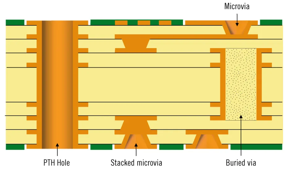
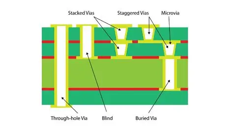
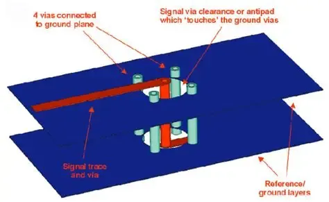
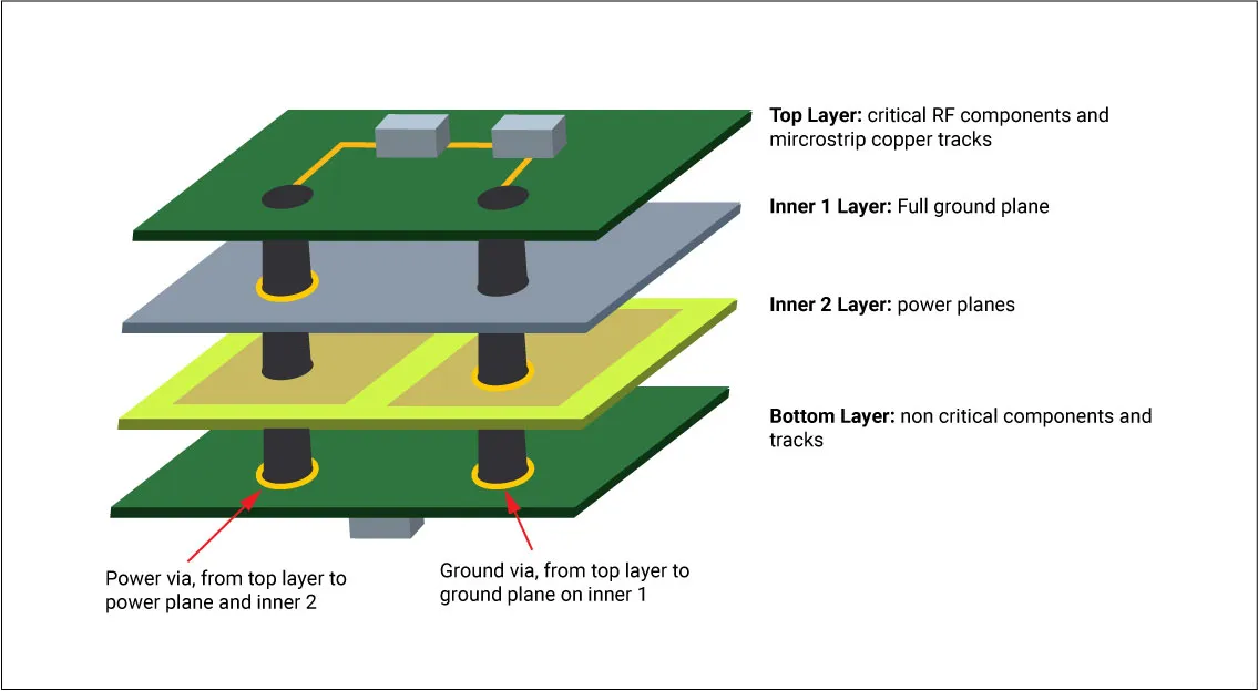
A continuous copper plane offers the lowest possible impedance for return currents at high frequencies. At these frequencies, return current tends to flow directly beneath the signal trace due to electromagnetic coupling, minimizing the current loop area. Any gaps, slots, or splits in the plane force the return current to detour, raising inductance and creating potential antennas for EMI. Differential pairs benefit from symmetric ground references on adjacent layers to maintain controlled impedance and reduce common-mode conversion. Via placement must also consider the plane as a reference; stitching vias connect multiple ground layers and provide additional low-inductance paths. Thermal relief connections around component pads should be evaluated to avoid introducing unintended discontinuities.
Impedance control relies on consistent dielectric thickness and plane proximity. Variations in plane coverage can alter the effective dielectric constant seen by high-speed signals. In addition, plane resonance can occur when board dimensions approach multiples of signal wavelengths, leading to peaks in radiated emissions. Proper plane segmentation, when necessary, should follow strict rules to avoid creating isolated islands that act as secondary radiators. These mechanisms are governed by fundamental electromagnetic principles rather than arbitrary layout choices.
DFM Ground Plane Strategies for Reliable Manufacturing
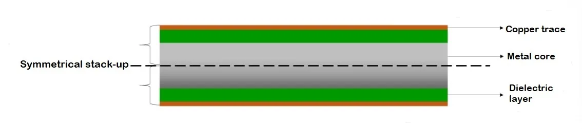
Design for manufacturability requires attention to copper distribution across all layers to prevent warpage during lamination and reflow. Large solid planes on one side of the board should be balanced with similar copper percentages on the opposite side. Cross-hatching or selective removal of copper in non-critical areas can help equalize coverage without sacrificing electrical performance. Minimum plane-to-edge clearances must comply with fabrication capabilities to avoid exposed copper or etching issues. Via fill and capping processes also interact with ground planes, as unfilled vias can create voids that affect both thermal and electrical behavior.
Signal return path optimization involves placing ground vias near signal layer transitions. These vias allow return current to follow the shortest path when signals change layers. The number and spacing of stitching vias depend on the maximum frequency content of the signals involved. Designers should also consider the impact of plane splits required for power distribution; any split must be bridged with sufficient stitching to maintain a low-impedance reference. Thermal management considerations may require additional copper areas connected to the ground plane, yet these additions must not create unintended current paths or resonance conditions.
Best Practices for EMI Reduction in High-Speed PCBs
Solid ground planes beneath critical high-speed signals provide the most effective shielding against both conducted and radiated EMI. Placing power planes adjacent to ground planes creates embedded decoupling capacitance that reduces noise on supply rails. Component placement should keep high-speed devices close to their associated ground vias to shorten return paths. Ground plane pours on outer layers can supplement inner planes but must maintain consistent clearance from signal traces to avoid impedance discontinuities. When multiple ground domains are required, careful isolation combined with controlled bridging prevents noise coupling between sections.
Testing and validation of ground plane effectiveness typically involve measuring radiated emissions in a controlled environment and verifying signal integrity through time-domain reflectometry and eye diagram analysis. Adjustments to plane geometry or via patterns are made iteratively based on these measurements. These practices align with established industry standards for board fabrication and performance qualification.
Troubleshooting Common Ground Plane Issues
Engineers often encounter excessive EMI when return paths are interrupted by dense via fields or component footprints. In such cases, adding dedicated ground vias or adjusting trace routing to avoid plane disruptions can restore performance. Board warpage caused by unbalanced copper may lead to assembly defects that indirectly affect grounding quality through poor solder joints. Reviewing layer stack-up symmetry early in the design cycle helps prevent these problems. Signal integrity problems traced to ground bounce can be mitigated by increasing the number of ground pins on connectors and ICs, thereby lowering the overall inductance of the return network.
Conclusion
Effective ground plane strategies integrate electrical performance requirements with manufacturing realities to achieve both signal integrity and EMI reduction in high-speed PCBs. Continuous planes, strategic via placement, and balanced copper distribution form the foundation of reliable designs. Attention to return path optimization throughout the layout process minimizes the need for corrective measures later in development. These approaches support consistent results across prototypes and production volumes while meeting applicable industry standards.
FAQs
Q1: How does ground plane design affect signal integrity in high-speed PCBs?
A1: A continuous ground plane provides a low-impedance return path that keeps current loops small and reduces inductance. Disruptions in the plane increase loop area, leading to higher crosstalk and reflections that degrade signal quality. Proper implementation supports consistent impedance and minimizes timing issues across the board.
Q2: What DFM ground plane strategies help minimize EMI?
A2: Balanced copper distribution prevents warpage while maintaining plane continuity. Strategic placement of stitching vias around any necessary splits ensures return currents follow low-inductance paths. These steps reduce radiated emissions without compromising manufacturability or assembly yield.
Q3: Why is signal return path optimization important for EMI reduction PCB designs?
A3: Return current follows the path of least inductance directly beneath the signal trace when a solid ground plane is present. Interruptions force longer paths that act as antennas and increase electromagnetic interference. Optimized paths therefore limit both conducted and radiated noise.
Q4: How many ground vias are typically needed near layer transitions?
A4: The number depends on signal frequency content and the size of any plane discontinuities. Multiple vias spaced appropriately provide parallel low-inductance paths for return current. Designers evaluate via count during layout to maintain acceptable impedance and emission levels.
References
IPC-2221B — Generic Standard on Printed Board Design. IPC, 2012
IPC-6012E — Qualification and Performance Specification for Rigid Printed Boards. IPC, 2017
JEDEC J-STD-020E — Moisture/Reflow Sensitivity Classification. JEDEC, 2014