ALLPCB


Introduction
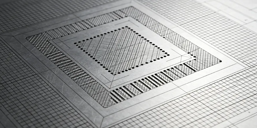
Step-up stencils play a critical role in surface mount technology processes where uniform solder paste deposition becomes challenging due to variations in component sizes or board topography. Engineers often encounter situations in which standard stencils fail to deliver adequate paste volume for larger pads or areas affected by slight board deformation. A step-up stencil addresses these issues by incorporating localized thickness increases that allow greater paste release without altering the overall stencil structure. This approach improves joint reliability for mixed-technology assemblies and reduces defects such as insufficient solder or bridging. Proper implementation requires careful attention to aperture geometry, pad alignment, and material selection to maintain process stability across production runs.
What Is a Step-Up Stencil and Why It Matters
A step-up stencil features selective thickening in specific regions, typically achieved through additive manufacturing or precision etching techniques that create raised areas aligned with target pads. This design differs from conventional flat stencils by enabling higher paste volumes exactly where needed while preserving finer apertures elsewhere on the same foil. In high-mix electronics manufacturing, the technique supports consistent printing for both small passive components and larger connectors or power devices on a single board. Industry professionals recognize its value in minimizing rework and enhancing first-pass yield when board warpage or component coplanarity variations are present. Effective use depends on integrating step-up stencil design software early in the layout phase to simulate paste release and identify potential conflicts before fabrication.
Technical Principles of Step-Up Stencil Design
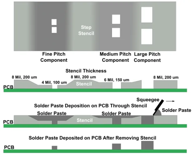
The underlying mechanism relies on controlled foil thickness transitions that increase the volume of solder paste transferred through enlarged apertures without compromising release characteristics. Engineers calculate the required step height based on target paste volume, typically expressed as a percentage of pad area, while ensuring the transition zones remain smooth to avoid paste scooping or incomplete release. Material properties such as foil hardness and surface finish directly influence how well the stencil maintains dimensional stability during repeated printing cycles. Thermal expansion differences between the stencil and substrate must also be considered, particularly when operating at elevated temperatures during reflow. Structured analysis of these factors helps predict long-term performance and supports consistent results across varying production environments.
Related Reading: Step Stencil Thickness: How to Determine the Ideal Value for Your PCB
Practical Solutions and Best Practices
Designers begin by defining step-up regions through detailed pad analysis, ensuring that aperture dimensions scale proportionally with the increased foil thickness to achieve the desired paste deposit. In step-up stencil aperture design, engineers apply aspect ratio guidelines that prevent clogging while maximizing transfer efficiency, often verifying results through test prints on representative substrates. Step-up stencil pad design requires precise alignment of the thickened zones with component footprints, including appropriate clearance to adjacent fine-pitch areas to avoid paste migration. When incorporating a step-up stencil keep-out area, teams establish buffer zones around the raised sections that prevent interference with squeegee travel or stencil tensioning hardware. A thorough step-up stencil design review follows, incorporating simulation outputs from step-up stencil design software to validate volume targets and identify any mechanical stress points before ordering the final stencil.
Considerations for Design Review and Process Integration
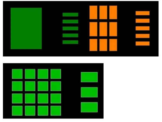
During the review phase, teams evaluate the interaction between step-up features and overall board layout, paying particular attention to keep-out distances that protect surrounding circuitry from excess paste. Engineers also assess stencil tension and support structures to ensure the raised areas do not introduce flexing that could affect print uniformity. Process parameters such as squeegee pressure, speed, and separation distance are adjusted iteratively based on feedback from trial runs, always maintaining traceability to established quality criteria. Documentation of each design decision supports reproducibility and facilitates future revisions when component or layout changes occur. This disciplined approach aligns with recognized industry standards such as those outlined in IPC-7525 for stencil design guidelines.
Related Reading: Mastering Step Up Stencils: A Comprehensive Guide for PCB Assembly
Conclusion
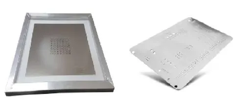
Step-up stencil implementation offers a targeted solution for achieving reliable solder paste volumes in complex assemblies when standard approaches prove insufficient. Success hinges on methodical aperture and pad design, combined with rigorous keep-out area planning and comprehensive design reviews supported by specialized software. Adherence to proven engineering practices ensures that the benefits of increased paste volume translate into improved joint quality and reduced defect rates. Organizations that integrate these considerations early in the development cycle consistently achieve more stable manufacturing outcomes across diverse product mixes.
FAQs
Q1: How does step-up stencil design software improve the overall process?
A1: Step-up stencil design software enables precise modeling of thickness transitions and aperture scaling before physical production begins. Engineers use the tool to calculate optimal paste volumes and verify alignment with component pads while identifying potential conflicts with fine-pitch areas. This simulation capability reduces trial-and-error iterations on the manufacturing floor and supports faster qualification of new designs.
Q2: What factors influence step-up stencil aperture design?
A2: Aperture design in a step-up stencil must balance increased paste volume against release efficiency and print definition. Key considerations include the aspect ratio between aperture width and foil thickness, the shape of the opening, and the smoothness of transitions at step boundaries. Proper sizing ensures adequate deposit for larger components without causing bridging or insufficient fill on adjacent pads.
Q3: Why is a step-up stencil keep-out area important during layout?
A3: A step-up stencil keep-out area prevents interference between the raised foil sections and surrounding features such as tooling holes, fiducials, or fine-pitch components. Maintaining adequate clearance protects stencil integrity during handling and printing while preserving uniform tension across the entire foil. This practice supports consistent squeegee contact and reduces the risk of localized defects.
Q4: When should a step-up stencil design review be performed?
A4: A step-up stencil design review should occur after initial aperture and pad definitions are complete but before stencil fabrication. The review incorporates simulation results, mechanical stress analysis, and process parameter validation to confirm that all design elements meet volume targets and quality requirements. Early completion of this step minimizes costly revisions later in the production cycle.
References
IPC-7525B — Stencil Design Guidelines. IPC, 2018
IPC-A-610G — Acceptability of Electronic Assemblies. IPC, 2017
J-STD-005A — Requirements for Soldering Pastes. IPC, 2016