 ALLPCB


Overview
In a non-discharging RCD snubber, the power dissipated in RSNB is limited to surge energy, so the allowable dissipation for RSNB can be relatively small. Therefore, the capacitance of CSNB can be increased, which not only improves clamping but also allows a higher switching frequency fSW.
Generally, adding a non-discharging RCD snubber reduces efficiency at light load and increases efficiency at heavy load. At heavy load, the snubber suppresses surges and can reduce switching loss.
This article describes the fourth and final snubber type: the non-discharging RCD snubber.
SiC MOSFET
Design of the non-discharging RCD snubber
Unlike the discharging RCD snubber, the power dissipated in RSNB of the non-discharging RCD snubber equals only the surge energy, allowing a smaller allowable dissipation for RSNB. This expands the selection options for RSNB and makes it possible to increase the capacitance of CSNB, improving clamping performance.
CSNB is determined by formula (2) in the section "C snubber design", and RSNB is determined by formula (3) in the section "RC snubber design". However, the power loss of RSNB is given by formula (6) below. Because formula (4) in "RC snubber design" does not include terms containing CSNB and fSW, there is basically no loss increase caused by CSNB and fSW. Therefore CSNB can be chosen with a larger capacitance, enabling a snubber with better clamping; this also supports increasing fSW.
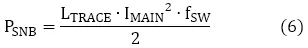
Figure 1 shows the discharge path after the non-discharging RCD snubber operates. The surge current from the upper half-bridge flows to PGND; the discharge current from the lower half-bridge flows through RSNB to HVdc, so it is less affected by wiring inductance. However, because the current change is large, the wiring inductance LSNB between the MOSFET drain and source should be kept as small as possible.
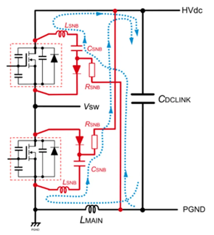
Figure 1. Discharge of the non-discharging RCD snubber
Waveforms used to verify the non-discharging RCD snubber with SiC MOSFET SCT3080KR on evaluation board P02SCT3040KR-EVK-001. Panel (a) is the test circuit; panel (b) shows turn-off waveforms with and without the snubber. Conditions: RG_EXT = 3.3 Ω, HVdc = 800 V, drain current ID ≈ 70 A for the turn-off waveform.
Without the snubber the turn-off surge reached 1210 V; with the snubber it was 1069 V, a reduction of about 12%. The snubber also eliminated the voltage ringing associated with the surge, which reduces EMI.
Figure 2 compares conversion efficiency in a buck converter. Conditions: Vin = 400 V, Vout = 200 V, RG_EXT = 6.8 Ω, switching frequency fSW = 100 kHz.
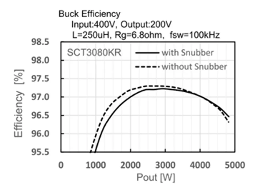
Figure 2. Efficiency of the buck circuit
When output power varies from 1 kW to 4.8 kW, below about 4 kW the efficiency without the snubber is up to 0.4% higher than with the snubber; above 4 kW the efficiency with the snubber is 0.15% higher than without it. This is because as load power increases, surge-induced losses (losses in capacitor equivalent series resistance caused by resonant currents) increase. By suppressing surges, the snubber reduces switching losses.


