 ALLPCB


Introduction
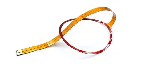
Flexible PCBs enable compact, lightweight designs in applications ranging from wearables to aerospace systems, where traditional rigid boards fall short. In flexible PCB design, trace clearance refers to the minimum distance between conductive traces, serving both electrical isolation and mechanical integrity purposes. Unlike rigid PCBs, flex circuits endure repeated bending, introducing unique stresses that demand careful spacing considerations. Factors like bending stress and material properties significantly influence flex PCB trace clearance requirements, particularly in high-density interconnect layouts. Engineers must balance density with reliability to prevent failures such as shorts or cracks. This article explores these challenges and provides structured solutions grounded in engineering principles.
Understanding Flex PCB Trace Clearance and Its Importance
Trace clearance in flexible PCBs ensures sufficient spacing to avoid electrical arcing, crosstalk, and manufacturing defects while accommodating dynamic flexing. In rigid boards, clearance primarily addresses voltage breakdown and fabrication tolerances, but flex PCB trace clearance must also mitigate mechanical strain from bending cycles. High-density interconnect designs push trace widths and spacings to limits, amplifying risks in compact assemblies. Bending stress concentrates at trace edges, potentially leading to copper fatigue or dielectric puncture over time. Material properties, such as the ductility of copper foils and flexibility of substrates, directly impact how clearances perform under repeated deformation. Adhering to established guidelines prevents field failures, ensuring long-term reliability in demanding environments.
Proper clearance management supports miniaturization without compromising signal integrity or power handling. For electric engineers, optimizing flex PCB trace clearance involves integrating electrical, thermal, and mechanical analyses early in the design phase. This approach aligns with industry standards that emphasize performance under real-world conditions. Neglecting these aspects can result in costly redesigns or product recalls.
Key Challenges in Maintaining Trace Clearance
Flexible PCBs face distinct challenges due to their ability to bend, which rigid boards do not encounter. Bending stress arises from tensile and compressive forces during flexure, with outer traces experiencing higher strain than inner ones. In high-density interconnect regions, reduced clearances exacerbate this, as closer traces amplify stress concentrations and increase short-circuit risks. Material properties play a critical role; substrates with lower modulus allow greater flex but may permit trace migration under prolonged stress. Dynamic applications, involving millions of bend cycles, accelerate fatigue cracking at trace interfaces.
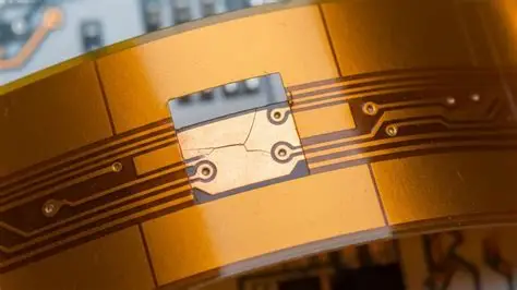
Manufacturing tolerances further complicate flex PCB trace clearance. Etching processes can undercut fine features, narrowing effective spacing in dense areas. Coverlay application adds variability, potentially bridging traces if not precisely aligned. Environmental factors, like humidity absorption in hygroscopic materials, alter dielectric strength, demanding conservative clearances. In multilayer flex stacks, interlayer alignment during lamination introduces risks of via-to-trace shorts.

High-density interconnect challenges intensify these issues. Microvias and fine-pitch traces reduce clearances to minimal levels, heightening sensitivity to bending-induced microcracks. Copper ductility varies with grain structure and annealing, affecting crack propagation rates. Engineers must model these interactions to predict failure modes accurately.
Engineering Mechanisms Behind Trace Clearance Issues
The primary mechanism driving clearance failures in flexible PCBs is mechanical strain during bending. When a flex circuit bends, the neutral axis remains unstressed, while outer layers elongate and inner layers compress. Traces positioned away from this axis experience proportional strain, with clearance gaps potentially closing under compression. Bending stress follows σ = E * ε, where modulus E and strain ε dictate local forces on copper. Parallel routing to the bend axis maximizes tensile stress along trace length, promoting hillock formation or fractures.
Material properties govern strain distribution. Adhesiveless laminates offer better copper-substrate adhesion, reducing delamination risks at trace edges. Dielectric materials with high elongation at break maintain spacing integrity longer. In high-density interconnects, thinner copper foils reduce overall stack stiffness but increase resistivity and electromigration under stress.
Fatigue from cyclic bending leads to progressive damage. Crack initiation occurs at trace edges due to stress risers, propagating inward and narrowing effective clearance. IPC-2223 provides guidelines for routing and spacing to minimize these effects in flex designs. Thermal expansion mismatches between copper and substrate further strain clearances during operation.
Vibration and shock in applications add dynamic loads, compounding bending stress. High-frequency signals in dense traces generate heat, softening materials and altering clearances locally.
Best Practices for Optimizing Flex PCB Trace Clearance
Engineers can address these challenges through targeted design strategies in flexible PCB design. Route traces perpendicular to the bend axis to distribute stress evenly across width, minimizing length-wise tension. Curved or teardrop-shaped transitions at pads reduce stress concentrations, preserving clearance uniformity. Increase spacing in anticipated high-strain zones, such as repeated flex areas, to accommodate deformation without bridging.
Material selection influences clearance robustness. Choose substrates with matched coefficients of thermal expansion to copper for stability. Thicker coverlay layers enhance dielectric protection in dense regions. For high-density interconnect, employ staggered via patterns to avoid crowding traces.
Simulation tools aid in predicting stress fields. Finite element analysis models bending radius, layer stackup, and trace geometry to optimize clearances iteratively. Prototype testing validates designs under accelerated cycles.
IPC-6013 outlines qualification tests for flex performance, including flex endurance that indirectly verifies clearance integrity. Incorporate strain-relief features like floating fingers or slack loops in dynamic zones.
Adhesives and stiffeners control bend radii, indirectly supporting trace spacing. Maintain consistent trace widths to avoid impedance variations that could induce currents stressing clearances.
Troubleshooting Common Flex Trace Clearance Failures
Electric engineers often encounter trace cracking in prototypes after initial flexing. Inspect for parallel routing or sharp corners, then redesign with perpendicular paths and fillets. Delamination signals poor adhesion; specify adhesiveless construction for critical areas.
Shorts in high-density interconnect sections stem from etch undercut. Verify fab capabilities for fine features and add test coupons. Bending radius violations cause bulk failures; enforce minimum radii based on stack thickness.
Field returns with intermittent opens point to fatigue. Analyze cycle counts and upgrade to higher-ductility copper. IPC-2221 informs baseline spacing for electrical reliability, adaptable to flex contexts.
Conclusion
Clearance between traces in flexible PCBs demands a holistic approach balancing electrical needs with mechanical demands. Unique challenges from bending stress and material properties necessitate tailored strategies like perpendicular routing and enhanced spacing in high-risk areas. High-density interconnect amplifies these, requiring precise modeling and testing. By following best practices and leveraging standards such as IPC-2223 and IPC-6013, engineers achieve robust designs. Prioritizing flex PCB trace clearance ensures product longevity and performance in dynamic applications.
FAQs
Q1: What factors most affect flex PCB trace clearance during bending?
A1: Bending stress, trace orientation relative to the bend axis, and material properties like copper ductility primarily influence clearance. Perpendicular routing distributes strain evenly, reducing crack risks in high-density interconnect areas. Substrate elongation maintains dielectric gaps under flexure. Engineers should model neutral axis positioning for optimal results.
Q2: How does high-density interconnect impact flexible PCB design?
A2: High-density interconnect reduces trace clearances, heightening vulnerability to bending stress and manufacturing defects. Finer pitches demand precise alignment and robust materials to prevent shorts. Flexible PCB design must incorporate microvias with adequate annular rings. This enables compact layouts while upholding reliability.
Q3: What are key solutions for managing bending stress in trace spacing?
A3: Use curved traces, teardrops at transitions, and wider clearances in flex zones to mitigate stress. Route perpendicular to bends and select ductile materials. Simulate strain distributions early. These practices align with flex PCB design guidelines for dynamic reliability.
Q4: Why consider material properties in flex PCB trace clearance?
A4: Material properties determine strain tolerance and dielectric strength under bending. High-modulus substrates resist deformation but crack sooner; flexible ones preserve spacing longer. Matching CTE minimizes thermal stresses. This ensures long-term integrity in high-density interconnect applications.
References
IPC-2221B — Generic Standard on Printed Board Design. IPC
IPC-2223C — Sectional Design Standard for Flexible/Rigid-Flex Printed Boards. IPC
IPC-6013D — Qualification and Performance Specification for Flexible and Rigid-Flex Printed Boards. IPC


