ALLPCB


Why EMI and EMC Matter in High-Frequency PCB Design
Electromagnetic interference arises when unintended energy couples between circuits or radiates into the environment, while electromagnetic compatibility ensures a board functions correctly within its electromagnetic surroundings. In high-frequency designs, shorter wavelengths increase the likelihood of radiation from traces, vias, and component leads. DFM practices help identify and mitigate these risks during layout and stack-up definition rather than after prototypes are built. Effective management supports stable operation in environments with multiple electronic systems operating simultaneously.
Technical Principles and Mechanisms of EMI Generation
High-frequency signals generate stronger electric and magnetic fields that can couple through capacitive and inductive paths. Trace impedance mismatches create reflections that amplify emissions, while poor return paths force currents to take longer routes and increase loop areas. Via transitions introduce discontinuities that excite higher-order modes, and component placement near board edges can enhance radiation efficiency. Ground planes with gaps or insufficient stitching allow fields to escape, turning the board into an unintended antenna. These mechanisms intensify as operating frequencies rise because wavelength decreases relative to board dimensions.
Material properties also influence behavior. Dielectric constant variations affect propagation velocity and can create resonances when combined with trace geometries. Copper roughness at high frequencies increases conductor losses and alters current distribution, contributing to localized heating and field distortion. Thermal expansion differences between layers may induce mechanical stress that indirectly affects electrical performance over time.
DFM Practices for Reducing Electromagnetic Interference
Designers apply DFM by establishing controlled impedance requirements early and verifying them against manufacturing tolerances. Trace width, spacing, and dielectric thickness are selected to match target impedances while remaining compatible with standard fabrication processes. Return paths are kept continuous and adjacent to signal layers to minimize loop inductance. Stitching vias connect reference planes at regular intervals to maintain low-impedance paths across the frequency range of interest.
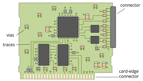
Shielding techniques in PCB design include dedicated ground planes, cavity shielding with conductive enclosures, and strategic placement of guard traces around sensitive lines. These measures contain fields within defined regions and reduce coupling to external circuits. Component orientation and grouping further support containment by aligning high-speed devices away from board edges and analog sections.
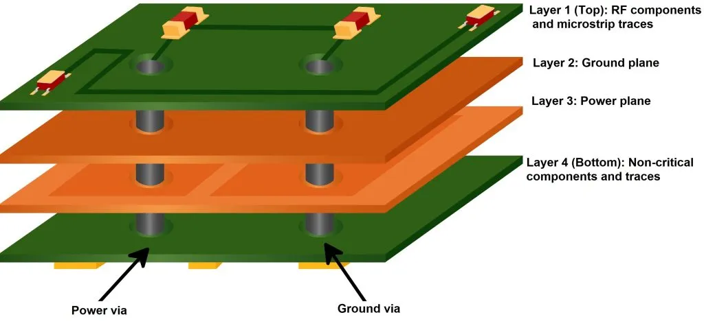
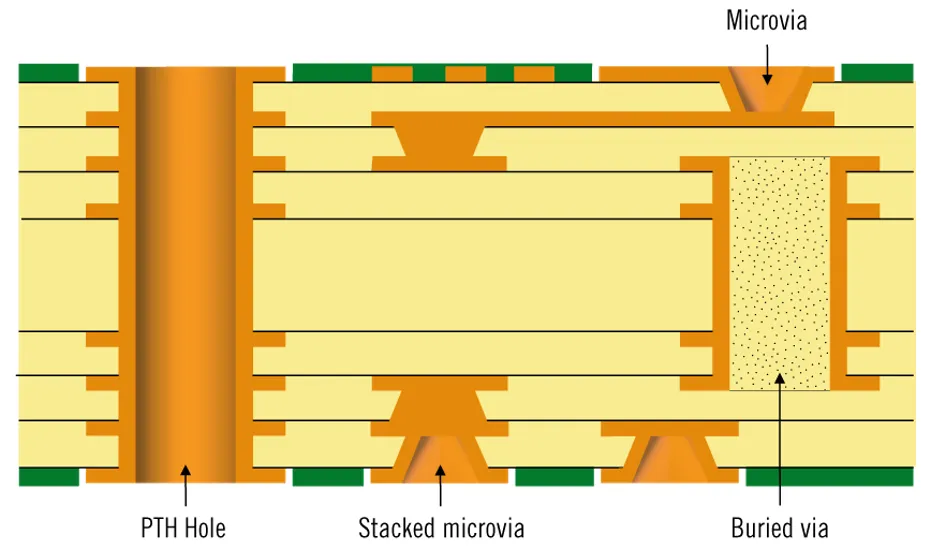
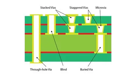
Stack-up planning forms a core DFM activity. Alternating signal and reference layers with appropriate thicknesses controls crosstalk and provides shielding between adjacent signals. Power distribution networks receive similar attention through plane capacitance and decoupling strategies that maintain low impedance across the operating bandwidth. Thermal relief patterns on planes are sized to avoid creating slots that could act as slot antennas.
Practical Implementation and Troubleshooting Insights
Layout reviews incorporate electromagnetic simulation checkpoints at key stages to validate that proposed geometries meet emission targets. Differential pair routing maintains tight coupling and equal lengths to cancel common-mode currents. Clock and data lines are routed on inner layers where possible to benefit from plane shielding. Test points and probe access are positioned to avoid disrupting return currents or introducing new discontinuities.
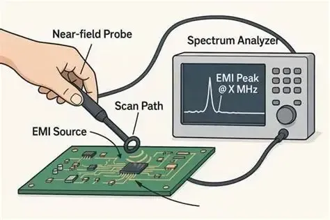
When issues appear during validation, systematic isolation begins with near-field probing to locate dominant sources. Adjustments such as adding stitching vias, modifying trace routing, or revising component placement are evaluated for manufacturability before implementation. These iterations remain within standard process capabilities to avoid yield impacts.
Conclusion
Integrating EMI and EMC considerations into DFM practices enables engineers to produce high-frequency PCBs that meet both electrical and manufacturing requirements. Structured attention to layout, stack-up, grounding, and shielding reduces emissions and improves immunity while preserving production efficiency. Consistent application of these methods supports reliable performance across product lifecycles.
FAQs
Q1: How do shielding techniques in PCB design help control EMI in high-frequency applications?
A1: Shielding techniques such as continuous ground planes, stitching vias, and guard traces contain electromagnetic fields and limit coupling between circuits. These methods reduce radiated emissions and improve immunity when applied during the DFM phase of high-frequency PCB development. Proper implementation maintains signal integrity without introducing manufacturing complications.
Q2: What role does DFM play in reducing electromagnetic interference in PCBs operating at high frequencies?
A2: DFM practices embed electromagnetic compatibility checks into layout and stack-up decisions, ensuring trace geometries, return paths, and material selections remain within fabrication tolerances. This proactive approach minimizes reflections, loop areas, and discontinuities that generate interference in high-frequency PCB designs.
Q3: Which industry standards guide EMI and EMC considerations during high-frequency PCB design?
A3: IPC-2221 provides generic guidance on printed board design parameters that influence electromagnetic performance. IEC 61000 series outlines electromagnetic compatibility testing and limits applicable to electronic assemblies including high-frequency PCBs.
Q4: How can engineers verify that DFM practices have effectively addressed EMI in a high-frequency PCB?
A4: Verification combines simulation of proposed layouts with physical measurements such as near-field scanning and compliance testing. Results are compared against design targets to confirm that grounding, shielding, and routing decisions have reduced interference sources to acceptable levels.
References
IPC-2221B — Generic Standard on Printed Board Design. IPC, 2012
IEC 61000 series — Electromagnetic Compatibility (EMC). IEC
IPC-6012E — Qualification and Performance Specification for Rigid Printed Boards. IPC, 2017