ALLPCB


Introduction
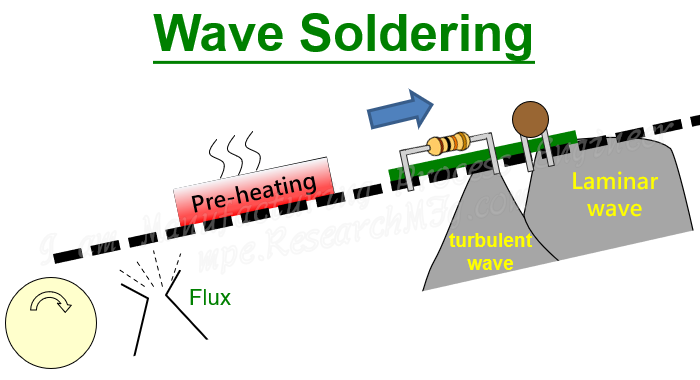
In PCB wave soldering, achieving uniform solder fillets remains a critical challenge for ensuring reliable through-hole assemblies. Solder fillets form the visible meniscus-shaped joints between component leads, plated through-holes, and pads, directly influencing mechanical strength and electrical performance. Variations in PCB wave soldering solder fillet shape or height can lead to weak joints prone to fatigue or vibration failure. Engineers must master process control to balance wetting, solder volume, and cooling for consistent results. This article explores practical strategies rooted in engineering principles and industry standards. By optimizing parameters like flux application and preheat, manufacturers can produce fillets that meet quality expectations every time.
Uniform solder fillets indicate proper solder flow and adhesion, essential for high-volume production. Poor control often results from inadequate surface preparation or mismatched machine settings, causing issues like insufficient wetting or bridging. Addressing these requires a systematic approach to process variables. Visual cues from the fillet provide immediate feedback on underlying dynamics such as surface tension and thermal profiles. For electric engineers troubleshooting assemblies, understanding these interactions unlocks repeatable quality.
What Are Solder Fillets in PCB Wave Soldering and Why Uniformity Matters
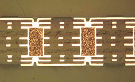
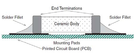
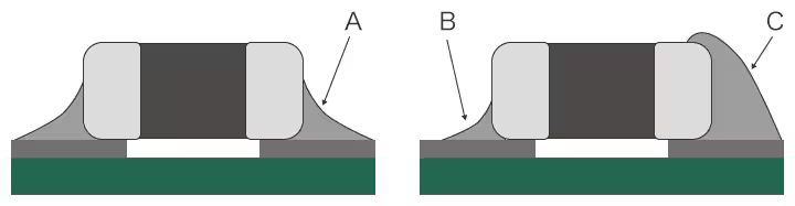
Solder fillets in PCB wave soldering refer to the curved solder mass that rises along the component lead and pad edges after the board passes over the molten solder wave. An ideal PCB wave soldering solder fillet exhibits a smooth, concave shape with full wetting on the lead, barrel, and pad surfaces. This formation depends on capillary action pulling solder into the through-hole and up the joint interfaces. Uniformity ensures each joint has comparable volume and contour, minimizing stress concentrations.
The relevance of uniform fillets stems from their role in joint integrity. Consistent PCB wave soldering fillet height, typically covering at least 75% of the exposed lead without excessive buildup, supports shear strength and thermal cycling reliability. Deviations signal problems like de-wetting or solder starvation, which compromise conductivity and increase failure rates in field use. IPC-A-610 provides criteria for assessing these features across assembly classes, guiding acceptability in production.
Engineers prioritize uniformity to streamline PCB wave soldering visual inspection, reducing scrap and rework. Fillets that vary across a panel often trace back to board warpage, component misalignment, or flux inconsistencies. Achieving balance enhances yield while meeting end-product specifications. In high-reliability applications, such as automotive or aerospace electronics, uniform fillets correlate directly with long-term performance.
Technical Principles of Solder Fillet Formation
Solder fillet development in wave soldering hinges on wetting dynamics, where molten solder spreads across metal surfaces via intermolecular forces. Flux removes oxides, enabling zero-force wetting balance that promotes even fillet buildup. Surface tension then shapes the meniscus, with optimal angles around 30 degrees indicating good adhesion. Imbalanced forces lead to convex or flat fillets, signaling poor PCB wave soldering wetting balance.
Thermal gradients play a key role, as the board's preheat influences solder viscosity and flow into holes. Insufficient preheat causes rapid cooling, trapping flux residues and hindering fillet formation. Conversely, overheating promotes excessive oxidation, distorting the PCB wave soldering fillet shape. Engineers monitor these via thermocouple profiles to maintain equilibrium.
Capillary action drives solder up the through-hole, filling 100% for robust barrels supporting the fillet. Plating quality on leads and holes affects this, with HASL or ENIG finishes influencing spread rates. Gravity and wave momentum further refine the contour during contact.
Viscosity changes with alloy composition, but process control standardizes outcomes regardless. J-STD-001 outlines requirements for these mechanisms, ensuring fillets withstand mechanical stresses.
Key Process Control Parameters for Uniform Fillets
Flux selection and application form the foundation, with low-solids, no-clean types applied via spray or foam for uniform coverage. Proper dwell time allows activation without residue buildup, directly impacting PCB wave soldering wetting balance. Over-application leads to bridging, while under-application causes dry joints with incomplete fillets.
Preheat zone control is next, targeting 100-150°C topside to expand holes and volatilize flux solvents. Multi-zone ovens provide ramp rates of 1-4°C/second, preventing thermal shock that warps boards and unevenly forms fillets. Consistent profiles across the panel ensure predictable solder interaction.
Solder pot temperature, held at 250-260°C for lead-free alloys, balances fluidity without dross formation. Wave parameters like height (3-6 mm) and lambda spacing optimize contact time of 2-5 seconds. Conveyor speed, typically 1-2 m/min, correlates inversely with dwell, fine-tuned for hole fill and fillet height.
Air knife positioning post-wave removes excess solder, refining PCB wave soldering fillet shape. Nitrogen blanketing reduces oxidation, yielding shinier, more uniform contours. Real-time monitoring via IR cameras flags deviations early.
- Flux Application: 500-1500 μg/cm2 — Impact: Wetting balance
- Preheat Topside Temp: 110-140°C — Impact: Hole fill uniformity
- Solder Temp: 255-265°C — Impact: Flow and shape
- Conveyor Speed: 1.0-1.8 m/min — Impact: Dwell time
- Wave Height: 4-5 mm — Impact: Solder volume
This list summarizes controls for quick reference in troubleshooting.
Optimizing PCB Wave Soldering Fillet Height and Shape
Fillet height emerges from solder volume and wetting extent, ideally rising 1.5 times the pad thickness above the board. Excessive height indicates overfill, risking cracks; insufficient height exposes leads to fatigue. Balancing via speed and wave adjustments achieves target profiles.
Shape perfection requires symmetric concave curves without spikes or hollows. Convex shapes point to de-wetting from contamination, while flat tops suggest cooling gradients. Flux chemistry and cleanliness dictate this symmetry.
PCB warpage control, via fixture or symmetric layouts, prevents tilting that skews heights across components. Post-solder cooling fans solidify shapes uniformly, avoiding slumping.
PCB Wave Soldering Visual Inspection and Quality Assurance
Visual inspection evaluates PCB wave soldering solder fillet completeness under 10x magnification per IPC-A-610. Criteria include 100% barrel fill, smooth heel and toe fillets, and no voids. Shininess and color uniformity confirm flux efficacy.
Automated optical systems scan for height variations, flagging outliers. Manual checks verify wetting angles and lead protrusion. Consistent training ensures inter-operator reliability.
Documentation of inspection data trends process drifts, enabling proactive tweaks.
Troubleshooting Common Issues with Solder Fillets
Insufficient fillet height often stems from high conveyor speeds reducing dwell. Slowing to 1.2 m/min or raising wave height resolves this, restoring volume. Dewetting shows as beading; clean stencils and fresh flux counteract it.
Bridging between pins requires mask dams or air knives. Uneven heights across panels signal warpage; pre-bend correction helps. Icicles form from turbulent waves; laminar flow nozzles fix this.
Solder balls indicate flux splash; lower spray pressure prevents them. Systematic logging isolates root causes.
Conclusion
Mastering uniform solder fillets in PCB wave soldering demands precise control of flux, preheat, and wave dynamics. These elements ensure optimal wetting balance, shape, and height for reliable joints. Regular visual inspection and troubleshooting sustain quality. Electric engineers benefit from standard-aligned practices like those in IPC-A-610 and J-STD-001. Implementing these yields higher first-pass yields and robust assemblies.
FAQs
Q1: What factors most affect PCB wave soldering fillet height?
A1: Preheat temperature, conveyor speed, and solder wave height primarily influence fillet height. Inadequate preheat limits hole fill, while excessive speed reduces dwell time for solder rise. Optimizing to 120°C topside and 1.5 m/min speed promotes uniform heights meeting acceptability criteria. Monitor via cross-sections for verification.
Q2: How does flux impact PCB wave soldering wetting balance?
A2: Flux removes oxides to enable proper wetting balance, allowing solder to spread evenly for concave fillets. Poor activation leads to de-wetting and irregular shapes. Select activators matching alloy and apply uniformly at 800 μg/cm2. Test via dip simulations before production runs.
Q3: What are ideal characteristics in PCB wave soldering visual inspection?
A3: During visual inspection, seek smooth, shiny fillets with full lead and barrel wetting, concave shapes, and heights covering pads adequately. Avoid cracks, voids, or excessive solder. Use 5-10x magnification per standards for consistent evaluation across classes.
Q4: How to correct poor PCB wave soldering fillet shape?
A4: Adjust preheat for better flux volatilization and solder pot temperature for optimal viscosity. Laminar waves prevent turbulence causing spikes. Nitrogen use enhances shape symmetry by minimizing oxidation. Profile boards post-adjustment to confirm improvements.
References
IPC-A-610H — Acceptability of Electronic Assemblies. IPC, 2019
IPC J-STD-001H — Requirements for Soldered Electrical and Electronic Assemblies. IPC, 2020