ALLPCB


Introduction
Etched SMT stencils play a key role in surface mount technology assembly by enabling precise application of solder paste onto printed circuit boards. For electronic hobbyists working on prototype projects or small batch builds, these tools offer a practical way to achieve consistent results without investing in high volume production equipment. An etched SMT stencil is typically created through a chemical process that forms apertures in a thin metal sheet, allowing paste to deposit accurately on pads. This approach supports reliable soldering during reflow, which helps reduce defects in assembled boards. Hobbyists often turn to this method when balancing cost with the need for functional prototypes.
What Is an Etched SMT Stencil and Why It Matters
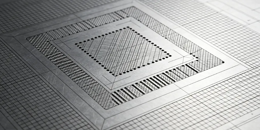
An etched SMT stencil consists of a stainless steel foil with openings patterned to match the solder paste requirements of a specific PCB layout. The chemical etching process removes material selectively to create these apertures, resulting in a low cost SMT stencil suitable for limited production runs. In contrast to other fabrication methods, this technique provides adequate precision for many hobbyist applications while keeping expenses manageable. Etched PCB stencils become particularly relevant when designers need to test circuit functionality before committing to larger orders. Their relevance grows in environments where quick iterations matter more than ultra fine feature sizes.
Technical Principles of Chemical Etching in SMT Stencils
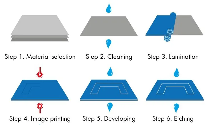
The chemical etching method relies on controlled exposure of a metal sheet to an etchant solution that dissolves unprotected areas, forming the desired aperture shapes. Engineers select foil thickness based on the volume of solder paste needed for each component pad, which directly influences deposit height and shape. This process allows for trapezoidal or other aperture profiles that aid paste release during printing. Industry standards such as J-STD-001 guide the overall soldering requirements that stencils must support for reliable joints. Proper alignment of the stencil with the board ensures paste lands only on designated pads, minimizing bridging or insufficient deposits.
Practical Considerations for Using Etched SMT Stencils
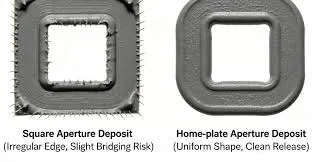
Hobbyists evaluating an etched SMT stencil for their project should first assess the component density and pad sizes on their PCB design. These stencils perform well for standard surface mount parts where aperture dimensions exceed roughly 0.2 millimeters, delivering acceptable paste volumes for reflow soldering. For finer features or high density layouts, users may encounter limitations in edge definition compared to alternative fabrication approaches. Practical testing on a sample board helps verify paste release and coverage before full assembly. Factors like squeegee pressure, printing speed, and stencil cleanliness also affect outcomes during manual or semi automated printing.
Best Practices and Troubleshooting for Prototype Work
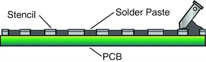
Start by ensuring the etched PCB stencil matches the PCB artwork exactly, including any fiducial marks for alignment. Clean the stencil thoroughly after each use to prevent dried paste from clogging apertures and causing inconsistent deposits on subsequent prints. When issues arise, such as incomplete paste release, adjusting the aperture aspect ratio or adding a slight taper during design review often resolves the problem. Monitoring environmental conditions like humidity helps maintain paste consistency, which supports repeatable results across multiple boards. These steps align with practical assembly guidelines found in standards such as IPC A 610 for evaluating final solder joint quality.
Conclusion
Etched SMT stencils provide electronic hobbyists with an accessible entry point into surface mount assembly for prototypes and low volume projects. Their chemical etching process balances cost and functionality for many common component types while supporting reliable solder paste application. Careful consideration of design features, printing parameters, and cleaning routines maximizes success rates. When project requirements stay within the capabilities of this stencil type, users achieve functional boards without unnecessary complexity. Overall, they represent a sound choice for those prioritizing affordability and practicality in early stage development.
FAQs
Q1: What distinguishes a chemical etched stencil from other SMT stencil types?
A1: A chemical etched stencil uses an etchant solution to create apertures in metal foil, offering a cost effective option for prototype SMT stencil needs. This method suits hobbyist projects where moderate precision meets volume requirements without advanced equipment. Users benefit from straightforward fabrication that supports standard component sizes effectively.
Q2: How does an etched SMT stencil support low cost PCB assembly?
A2: An etched SMT stencil enables precise solder paste deposition at a lower price point than alternatives, making it ideal for small runs and hobbyist builds. The process reduces material waste while delivering consistent results for typical surface mount components. Hobbyists often find it aligns well with budget constraints during iterative design phases.
Q3: When should a beginner choose an etched PCB stencil for their project?
A3: Beginners benefit from an etched PCB stencil when working with standard pad sizes and moderate component densities on prototype boards. It provides reliable paste application for reflow processes without requiring specialized tools. Evaluation of layout complexity helps determine suitability before committing to production.
Q4: What maintenance ensures consistent performance from a low cost SMT stencil?
A4: Regular cleaning after printing sessions prevents paste buildup that could affect aperture function in a low cost SMT stencil. Proper storage away from contaminants maintains foil integrity over multiple uses. Following basic handling practices supports repeatable results across hobbyist assembly tasks.
References
J-STD-001 — Requirements for Soldered Electrical and Electronic Assemblies. IPC, current revision
IPC-A-610 — Acceptability of Electronic Assemblies. IPC, current revision
ISO 9001:2015 — Quality Management Systems. ISO, 2015