 ALLPCB


Introduction
High-speed digital designs demand precise control over signal propagation to prevent degradation from reflections, crosstalk, and electromagnetic interference. An 8-layer PCB offers expanded routing channels, dedicated reference planes, and improved isolation, making it ideal for integrating multiple high-speed interfaces such as DDR4 memory, PCIe links, and USB 3.0 ports. These configurations allow engineers to maintain signal integrity at high speeds while accommodating dense component placement. This article examines the principles behind 8-layer PCB design, focusing on key aspects like DDR4 routing, PCIe layout, USB 3.0 design, signal integrity, and impedance matching. Through structured explanations and a practical case study, readers gain insights into optimizing performance without compromising reliability.
Why 8-Layer PCBs Matter in High-Speed Digital Design
An 8-layer PCB consists of eight conductive copper layers alternated with dielectric materials, providing four signal layers and four plane layers in typical configurations. This structure surpasses 4- or 6-layer boards by offering more space for differential pairs and controlled impedance traces, essential for data rates exceeding several gigabits per second. In high-speed applications, fewer layers often lead to longer traces, increased vias, and inadequate return paths, resulting in signal distortion. 8-layer designs mitigate these issues through symmetric stackups that minimize warpage and ensure balanced thermal expansion. Industry relevance stems from the proliferation of interfaces like DDR4 at 3200 MT/s, PCIe Gen4 at 16 GT/s, and USB 3.0 at 5 Gbps, where even minor layout flaws can cause bit errors or compliance failures. Engineers select 8-layer PCBs when routing density and electromagnetic compatibility become limiting factors in simpler boards.
The economic justification for 8 layers arises from reduced redesign iterations and faster time-to-market in competitive sectors like computing and telecommunications. Without sufficient layers, high-speed signals suffer from increased insertion loss and jitter, necessitating costly simulations or prototypes. 8-layer boards support advanced topologies, such as fly-by for DDR4, while dedicating inner layers to power distribution. This layered approach aligns with per IPC-2221 standards for controlled impedance and high-speed logic design, ensuring predictable electrical behavior. Ultimately, the choice elevates from performance needs rather than arbitrary complexity.
Key Technical Principles in 8-Layer PCB Design
Stackup Configuration for Signal Integrity
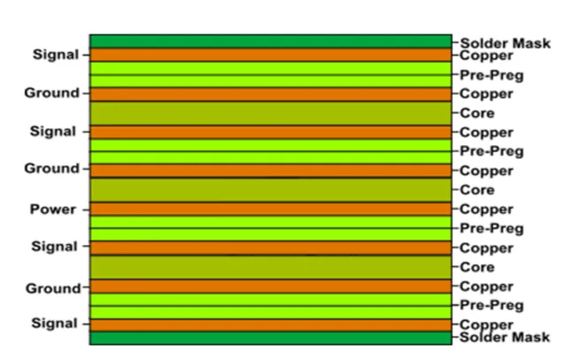
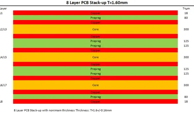
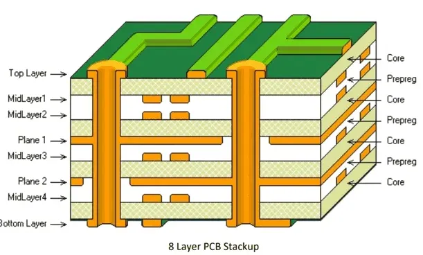
The foundation of an 8-layer PCB lies in its stackup, which dictates impedance, crosstalk, and return current paths. A common high-speed stackup places signal layers adjacent to ground planes: Layer 1 (top signal), Layer 2 (ground), Layer 3 (signal), Layer 4 (power), Layer 5 (power), Layer 6 (signal), Layer 7 (ground), Layer 8 (bottom signal). This arrangement confines fields between signal and reference planes, reducing radiation and broadening the signal bandwidth. Dielectric thicknesses between layers control characteristic impedance, typically targeting 50 ohms for single-ended and 90-100 ohms for differential pairs used in DDR4, PCIe, and USB 3.0. Symmetric core and prepreg selections prevent bow and twist, maintaining layer alignment during lamination
.
Impedance variations arise from material properties like dielectric constant (Dk) around 3.5-4.5 for FR-4 equivalents and loss tangent (Df) below 0.005 at gigahertz frequencies. Engineers calculate trace width, spacing, and height using field solvers to achieve tolerances within 10%. Poor stackup symmetry leads to via stub resonances, attenuating signals above 5 GHz.
Signal Integrity Challenges at High Speeds
8-layer PCB signal integrity at high speeds hinges on managing reflections, crosstalk, and losses. Reflections occur from impedance discontinuities at vias, bends, or connectors, quantified by return loss exceeding 10 dB up to the fundamental frequency. Crosstalk between adjacent differential pairs demands edge-coupled routing with spacing at least 3-5 times the trace width. For frequencies above 1 GHz, skin effect confines currents to trace surfaces, increasing effective resistance and attenuating signals. Vias introduce inductance and capacitance; blind or buried vias minimize stubs in critical nets. Pre-emphasis and equalization compensate for channel losses in PCIe and USB 3.0, but PCB layout must support low-loss paths.
Power integrity complements signal performance by providing stable voltage rails through dedicated planes split judiciously to avoid slots under high-speed traces. Decoupling capacitors placed near ICs filter noise, with via fences enhancing isolation.
Best Practices for High-Speed Routing and Layout
8-Layer PCB DDR4 Routing
DDR4 routing on 8-layer PCBs requires length-matched differential pairs with total skew under 10 ps per byte lane. Fly-by topology connects the controller to multiple ranks via stubs shorter than 0.5 inches to limit ringing. Route data (DQ/DQS) and address/command on inner signal layers adjacent to ground for tight impedance control at 100 ohms differential. Avoid 90-degree bends; use 45-degree miters or curves to preserve impedance. Per JEDEC standards, clock lines need phase alignment within 50 ps. Vias should employ backdrilling for lengths over 20 mils to eliminate stubs.
8-Layer PCB PCIe Layout
PCIe layout demands continuous reference planes under lanes, with trace lengths matched within 5 mils across transmitter to receiver. Gen3/4 signals at 8-16 GT/s require 100-ohm differential impedance and serpentine tuning for equalization. Route lanes as broadside coupled on adjacent layers if coplanar space is limited, maintaining 4-6 H spacing (H as dielectric height). Lane breaks over splits need stitching capacitors. Pre-layout simulations verify eye diagrams opening to 0.2 UI at BER 10^-12.
8-Layer PCB USB 3.0 Design and Impedance Matching
USB 3.0 SuperSpeed pairs target 90-ohm differential impedance with 85-100 ps skew tolerance. Route SSTX/SSRX on dedicated layers, minimizing vias and length to under 12 inches. Impedance matching involves precise width (5-7 mils) and gap (6-8 mils) calculations based on stackup. Shielding vias along edges reduce radiated emissions. Full-speed pairs can share layers but require guard traces. Test coupons on panels verify impedance via TDR before fabrication.
General impedance matching across protocols uses consistent reference planes and avoids mixing signal types on layers. Fabricate test structures per IPC-TM-650 methods for validation.
Case Study: High-Speed Digital Controller Board
Consider a digital controller board integrating a processor with DDR4-3200 memory, PCIe Gen4 x16, and dual USB 3.0 ports on an 8-layer PCB. Initial 6-layer attempts failed simulations due to crosstalk exceeding -30 dB and eye closure from via stubs. Migrating to 8 layers enabled Layer 3/6 for DDR4 fly-by nets (total etch 8 inches, matched to 0.5 mil), Layer 2/7 grounds providing return paths. PCIe lanes occupied Layer 1/8 outer pairs, backdrilled blind vias reducing stub length to 10 mils, achieving IL < 10 dB at 8 GHz.
USB 3.0 traces on Layer 6 used edge-coupled routing with 90-ohm Zdiff, separated 10 mils from DDR4. Power planes on Layers 4/5, split for 1.2V/3.3V domains, included 20 nF caps every 1 cm. Post-layout SI analysis showed DDR4 eye height 700 mV at 1.6 GHz, PCIe margins met Gen4 specs. Fabrication per IPC-6012 ensured Class 3 quality, with fab TDR confirming 100-ohm tolerance ±5%. Field tests confirmed error-free operation at full speeds, validating the design.
Challenges included warpage from asymmetric copper; resolved via balanced stackup. This case underscores 8-layer PCB impedance matching and layout precision for multi-protocol integration.
Conclusion
8-layer PCBs excel in high-speed digital design by providing robust stackups, precise routing for DDR4, PCIe, and USB 3.0, and superior signal integrity. Key principles like adjacent plane referencing and impedance control directly address gigabit challenges. Best practices in length matching, via optimization, and verification ensure compliance. The case study illustrates real-world gains in performance and reliability. Engineers should prioritize symmetric designs and standard adherence for optimal results. Future designs may evolve with higher layer counts, but 8 layers remain a versatile benchmark.
FAQs
Q1: What stackup is recommended for 8-layer PCB DDR4 routing?
A1: A symmetric 1-2-3-4-5-6-7-8 configuration with signals on odd layers adjacent to ground on even layers supports DDR4's 100-ohm differential pairs. This minimizes loop inductance and crosstalk. Route fly-by topologies on inner layers for isolation. Verify with stackup calculators targeting Dk 4.0. JEDEC guidelines ensure timing margins.
Q2: How does 8-layer PCB PCIe layout improve signal integrity at high speeds?
A2: Dedicated ground planes under PCIe lanes confine fields, reducing EMI and enabling 16 GT/s operation. Backdrilled vias eliminate stubs, preserving eye quality. Length matching within 5 mils across links prevents skew. Simulations confirm low insertion loss and return loss.
Q3: Why is impedance matching critical in 8-layer PCB USB 3.0 design?
A3: Matching to 90 ohms prevents reflections that degrade SuperSpeed signals at 5 Gbps. Stackup dielectric heights dictate trace geometry for ±10% tolerance. Continuous references avoid discontinuities. TDR validation post-fab confirms integrity.
Q4: When should engineers choose an 8-layer PCB for high-speed signals?
A4: Opt for 8 layers when 6-layer routing exceeds density limits or signal integrity fails, as in DDR4/PCIe/USB combinations. It provides plane pairs for PDN stability and isolation. Balanced designs per IPC standards minimize warpage.
References
IPC-2221B — Generic Standard on Printed Board Design. IPC, 2012
IPC-6012E — Qualification and Performance Specification for Rigid Printed Boards. IPC, 2017
JEDEC JESD79-4 — DDR4 SDRAM Standard. JEDEC, 2012
IPC-TM-650 — Test Methods Manual. IPC, latest


