 ALLPCB


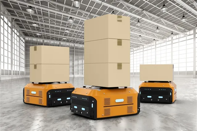
In the fast-paced world of warehouse automation, autonomous robots are revolutionizing how goods are moved, sorted, and managed. At the heart of these intelligent machines lies a critical component: the Printed Circuit Board (PCB). These intricate boards power the navigation systems, sensors, and communication modules that enable robots to operate without human intervention. Specifically, innovations in PCB design for LiDAR sensors in warehouse robots, PCB layout for SLAM algorithms, PCB for autonomous navigation systems, PCB for obstacle detection systems, and wireless communication PCB for warehouse robots are driving this transformation. In this blog, we’ll explore how these PCB advancements are shaping the future of warehouse robotics, providing actionable insights for engineers and tech enthusiasts.
Why PCBs Are the Backbone of Warehouse Robots
Warehouse robots rely on a complex network of sensors, processors, and communication systems to navigate dynamic environments, avoid obstacles, and communicate with central systems. PCBs serve as the foundation for integrating these components, ensuring seamless data flow and real-time decision-making. Without optimized PCB designs, robots would struggle with latency issues, inaccurate sensor readings, or unreliable wireless connections—problems that could halt warehouse operations.
Modern PCB innovations focus on miniaturization, high-speed signal processing, and power efficiency to meet the demands of autonomous navigation. Whether it's enabling LiDAR sensors to map surroundings or supporting SLAM (Simultaneous Localization and Mapping) algorithms for precise positioning, PCBs are the unsung heroes behind every autonomous move a robot makes.
PCB Design for LiDAR Sensors in Warehouse Robots
LiDAR (Light Detection and Ranging) sensors are a cornerstone of autonomous navigation in warehouse robots. These sensors use laser pulses to create detailed 3D maps of the environment, allowing robots to detect obstacles and plan paths with precision. However, LiDAR systems generate massive amounts of data that require rapid processing, making PCB design for LiDAR sensors in warehouse robots a critical focus area.
A well-designed PCB for LiDAR must prioritize high-speed signal integrity to handle data rates often exceeding 1 Gbps. This involves using low-loss dielectric materials and maintaining controlled impedance—typically around 50 ohms for high-frequency signals—to prevent signal degradation. Additionally, noise reduction techniques, such as strategic placement of decoupling capacitors near power pins, are essential to ensure accurate sensor readings.
Thermal management is another key consideration. LiDAR systems can generate significant heat during continuous operation, so PCBs often incorporate heat sinks or thermal vias to dissipate heat effectively. By optimizing the PCB layout, engineers can ensure that LiDAR sensors operate reliably even in the demanding conditions of a busy warehouse.
PCB Layout for SLAM Algorithms
SLAM algorithms allow warehouse robots to build maps of unknown environments while simultaneously determining their own location within those maps. This technology is vital for robots operating in dynamic settings where pre-programmed paths are impractical. The PCB layout for SLAM algorithms plays a pivotal role in ensuring the computational power and sensor integration needed for real-time processing.
SLAM requires a PCB design that supports high-performance microprocessors or GPUs capable of handling complex calculations at speeds of up to 100 MHz or more. These processors must communicate with multiple sensors—such as LiDAR, cameras, and inertial measurement units (IMUs)—without latency. To achieve this, engineers use multi-layer PCBs with dedicated ground planes to minimize electromagnetic interference (EMI) and ensure clean power delivery.
Moreover, the PCB layout must account for tight spacing constraints in compact robot designs. By using high-density interconnect (HDI) technology, designers can pack more components into smaller spaces, enabling efficient integration of SLAM hardware. This ensures that robots can process environmental data and adjust their movements in milliseconds, avoiding collisions and optimizing routes.
PCB for Autonomous Navigation Systems
Autonomous navigation systems are the brains that guide warehouse robots through crowded aisles and unpredictable environments. These systems integrate data from various sources—sensors, algorithms, and external inputs—to make split-second decisions. The PCB for autonomous navigation systems must be designed to handle this complexity while maintaining reliability and efficiency.
One key aspect of these PCBs is power management. Autonomous robots often operate for long shifts, requiring efficient voltage regulation to minimize energy loss. For instance, a typical navigation system might operate at 3.3V or 5V, with current demands ranging from 500 mA to 2 A depending on the workload. PCBs with integrated DC-DC converters and low-dropout (LDO) regulators help maintain stable power delivery, extending battery life.
Additionally, these PCBs must support real-time operating systems (RTOS) that prioritize critical navigation tasks. This requires careful routing of high-speed data lines to avoid crosstalk, often achieved by maintaining a signal-to-noise ratio (SNR) above 20 dB. By focusing on these design elements, engineers can create PCBs that enable flawless navigation, even in the most challenging warehouse layouts.

PCB for Obstacle Detection Systems
Obstacle detection is a non-negotiable feature for warehouse robots, ensuring they avoid collisions with objects, people, and other robots. Systems like ultrasonic sensors, infrared detectors, and LiDAR work together to identify potential hazards in real time. The PCB for obstacle detection systems must be meticulously designed to support these sensors and ensure rapid response times.
A primary challenge in designing these PCBs is managing mixed-signal environments. Obstacle detection systems often combine analog sensor inputs with digital processing, requiring careful separation of analog and digital ground planes to prevent noise interference. For example, analog signals from ultrasonic sensors might operate at frequencies below 100 kHz, while digital processing occurs at much higher speeds, necessitating isolation to avoid signal distortion.
Furthermore, obstacle detection PCBs must be compact yet robust, as they are often integrated into space-constrained robot designs. Using surface-mount technology (SMT) components and optimizing trace widths—typically around 6-8 mils for signal lines—helps achieve this balance. The result is a reliable system that allows robots to stop or reroute within milliseconds of detecting an obstacle.

Wireless Communication PCB for Warehouse Robots
In a modern warehouse, robots don't operate in isolation—they communicate with central control systems, other robots, and IoT devices to coordinate tasks. This connectivity is made possible by wireless communication PCB for warehouse robots, which supports protocols like Wi-Fi, Bluetooth, and Zigbee for seamless data exchange.
Designing PCBs for wireless communication requires a focus on radio frequency (RF) performance. This includes matching the impedance of RF traces—often set at 50 ohms—to the antenna to maximize signal strength. Additionally, engineers must minimize EMI by using shielding techniques and placing RF components away from high-noise areas of the board.
Power efficiency is also critical, as wireless modules can consume significant energy. For instance, a Wi-Fi module might draw 200-300 mA during active transmission, so integrating power-saving modes into the PCB design helps conserve battery life. These optimizations ensure that robots maintain constant communication, receiving real-time updates on inventory, orders, and traffic within the warehouse.
Challenges in PCB Design for Warehouse Robotics
While PCB innovations are driving autonomous navigation, several challenges remain. One major issue is balancing cost with performance. High-speed materials and HDI designs, while effective, can increase manufacturing costs, which may be a barrier for scaling production. Engineers often need to find creative solutions, such as hybrid layouts that combine standard and advanced materials, to keep expenses manageable.
Another challenge is ensuring durability. Warehouse environments can be harsh, with vibrations, temperature fluctuations, and dust affecting PCB performance. Using conformal coatings and robust soldering techniques can help protect boards, extending their lifespan to 5-10 years even under tough conditions.
Finally, the rapid pace of technology means PCBs must be future-proof. Modular designs that allow for easy upgrades—such as adding new sensor interfaces or communication protocols—are becoming increasingly popular. This adaptability ensures that warehouse robots remain competitive as new navigation technologies emerge.
The Future of PCB Innovations in Warehouse Automation
Looking ahead, the role of PCBs in warehouse robotics will only grow. Advances in artificial intelligence (AI) and machine learning (ML) will demand even more processing power, pushing PCB designs toward higher densities and faster signal speeds. For example, future PCBs might need to support data rates of 10 Gbps or more to handle AI-driven navigation algorithms.
Additionally, the integration of 5G technology into wireless communication PCBs will enable ultra-low latency connections, allowing robots to respond to commands in less than 1 millisecond. This could transform warehouse operations, enabling fleets of robots to work in perfect sync, maximizing efficiency.
Sustainability is also becoming a focus. Engineers are exploring eco-friendly PCB materials and recycling processes to reduce the environmental impact of manufacturing. These trends highlight the exciting potential of PCBs to not only enhance robot performance but also contribute to greener, smarter warehouses.
Conclusion: Powering the Future with PCB Excellence
PCBs are the silent force behind the autonomous navigation of warehouse robots, enabling everything from LiDAR mapping to obstacle detection and wireless communication. Innovations in PCB design for LiDAR sensors in warehouse robots, PCB layout for SLAM algorithms, PCB for autonomous navigation systems, PCB for obstacle detection systems, and wireless communication PCB for warehouse robots are paving the way for smarter, more efficient operations. By focusing on high-speed signal integrity, power efficiency, and compact designs, engineers can create PCBs that meet the rigorous demands of modern automation.
As technology continues to evolve, staying ahead of the curve with cutting-edge PCB solutions will be essential for any warehouse looking to optimize its robotic workforce. With the right designs, the brains behind the bots will keep pushing the boundaries of what's possible, transforming warehouses into hubs of precision and productivity.


