 ALLPCB


In the fast-paced world of high-speed PCB design, maintaining signal integrity is a top priority. One powerful solution to achieve this is by using stacked vias. But how do stacked vias help with stacked via signal integrity, and why are they critical for modern circuits? In short, stacked vias reduce signal loss, improve impedance control, and provide a better return path for high-speed signals, ensuring your designs perform at their best. This blog takes a deep dive into the benefits, implementation, and best practices of using stacked vias, offering actionable insights for PCB designers looking to optimize their high-speed designs.
What Are Stacked Vias and Why Do They Matter in PCB Design?
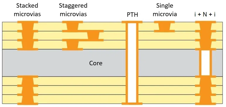
Stacked vias are a type of via structure in printed circuit boards (PCBs) where multiple vias are vertically aligned and connected through different layers of the board. Unlike traditional through-hole vias that span the entire board thickness or staggered vias that are offset, stacked vias are directly placed on top of each other, often in high-density interconnect (HDI) designs. They are typically used in multilayer PCBs to save space and improve electrical performance.
In high-speed PCB design, signal integrity is everything. As signal frequencies increase—often exceeding 1 GHz in modern applications—issues like signal loss, crosstalk, and impedance mismatches become more pronounced. This is where high-speed PCB design stacked via structures shine. Stacked vias help by minimizing the inductance and resistance in signal paths, ensuring cleaner signal transmission and reducing electromagnetic interference (EMI).
How Stacked Vias Improve Signal Integrity
Signal integrity refers to the quality of an electrical signal as it travels through a PCB. Poor signal integrity can lead to data errors, timing issues, and overall system failure. Stacked vias play a crucial role in addressing these challenges, particularly in high-speed designs. Let’s explore how they boost stacked via signal integrity.
1. Reducing Signal Loss
One of the biggest challenges in high-speed designs is signal loss, often caused by long signal paths or parasitic effects like inductance and capacitance. Stacked vias help in minimizing signal loss with stacked vias by shortening the connection between layers. For example, in a 12-layer PCB running signals at 5 GHz, a stacked via structure can reduce the signal path length by up to 30% compared to staggered vias, significantly lowering loss due to resistance.
Additionally, stacked vias are often paired with microvias, which have smaller diameters (typically 0.1 mm to 0.15 mm). This smaller size further reduces parasitic capacitance, ensuring that high-frequency signals maintain their strength over longer distances.
2. Enhancing Impedance Control
Impedance mismatches can cause signal reflections, leading to data corruption in high-speed circuits. Achieving stacked via impedance control is critical for maintaining a consistent impedance along the signal path. Stacked vias, when designed with proper dimensions and dielectric materials, help maintain a uniform characteristic impedance—often targeted at 50 ohms for single-ended signals or 100 ohms for differential pairs.
For instance, by using a dielectric material with a low dielectric constant (Dk) of around 3.5 and ensuring via diameters are optimized, designers can minimize impedance discontinuities. Tools like field solvers can simulate the impedance of a stacked via structure, allowing for fine-tuning before fabrication.
3. Optimizing Return Paths
A proper return path is essential for high-speed signals to avoid EMI and signal distortion. The stacked via return path offers a direct and low-inductance route for return currents, especially when placed near ground planes. In contrast, staggered vias or poorly placed through-hole vias can create longer return paths, increasing loop inductance and noise.
For example, in a design with a 10 Gbps data rate, a poorly optimized return path can introduce jitter of up to 10 ps. By using stacked vias adjacent to ground planes, this jitter can be reduced by aligning the return current path directly with the signal path, minimizing interference.
Benefits of Stacked Vias in High-Speed PCB Design
Stacked vias are particularly valuable in high-speed PCB design stacked via applications. Here are some key benefits that make them a go-to choice for modern PCB designers:
- Space Efficiency: Stacked vias take up less board space compared to staggered vias, making them ideal for compact HDI designs in devices like smartphones and IoT gadgets.
- Improved Performance: By reducing inductance and capacitance, stacked vias support higher signal frequencies, often exceeding 10 GHz, without significant degradation.
- Better Thermal Management: Stacked vias can also aid in heat dissipation when connected to thermal planes, enhancing the reliability of high-power components.
- Reduced Crosstalk: Their vertical alignment minimizes coupling between adjacent signal traces, reducing crosstalk by up to 20% in dense layouts.
Challenges and Best Practices for Implementing Stacked Vias
While stacked vias offer significant advantages, they come with challenges that PCB designers must address to ensure optimal performance. Below are some common hurdles and best practices for using stacked vias effectively.
Challenges with Stacked Vias
- Manufacturing Complexity: Stacked vias require precise alignment during fabrication, especially when using multiple microvias. Misalignment can lead to open circuits or reliability issues.
- Cost Implications: The process of creating stacked vias, often involving laser drilling for microvias, can increase manufacturing costs compared to traditional via structures.
- Reliability Concerns: Repeated thermal cycling in high-temperature environments can stress stacked vias, potentially causing cracks or delamination if not designed properly.
Best Practices for Stacked Via Design
To overcome these challenges and maximize the benefits of stacked vias, follow these actionable tips:
- Use Appropriate Aspect Ratios: Maintain a via aspect ratio (depth to diameter) of less than 0.8:1 for microvias in stacked structures to ensure reliable plating and avoid voids. For example, a 0.1 mm diameter microvia should not exceed 0.08 mm in depth per layer.
- Place Ground Planes Strategically: Position ground planes near stacked vias to provide a low-impedance stacked via return path. This reduces EMI and improves signal integrity at frequencies above 1 GHz.
- Simulate Before Fabrication: Use simulation tools to model the electrical behavior of stacked vias. Focus on impedance, signal loss, and return path optimization to catch issues early.
- Collaborate with Fabricators: Work closely with your PCB manufacturer to ensure they can achieve the required precision for stacked via alignment and plating. Specify tolerances clearly in your design files.
- Opt for Low-Loss Materials: Choose dielectric materials with a low dissipation factor (Df) of less than 0.005 to complement stacked vias in minimizing signal loss with stacked vias. This is especially critical for signals above 5 GHz.
Applications of Stacked Vias in Modern Electronics
Stacked vias are widely used in industries where high-speed and high-density designs are non-negotiable. Some common applications include:
- Telecommunications: In 5G infrastructure, stacked vias enable high-frequency signal routing with minimal loss, supporting data rates of up to 25 Gbps.
- Consumer Electronics: Devices like tablets and wearables rely on HDI designs with stacked vias to fit complex circuitry into tiny form factors.
- Automotive Systems: Advanced driver-assistance systems (ADAS) use stacked vias to handle high-speed sensor data with low latency and high reliability.
- Data Centers: Servers and networking equipment use stacked vias to manage high-speed interconnects, ensuring error-free data transmission at speeds exceeding 10 Gbps.
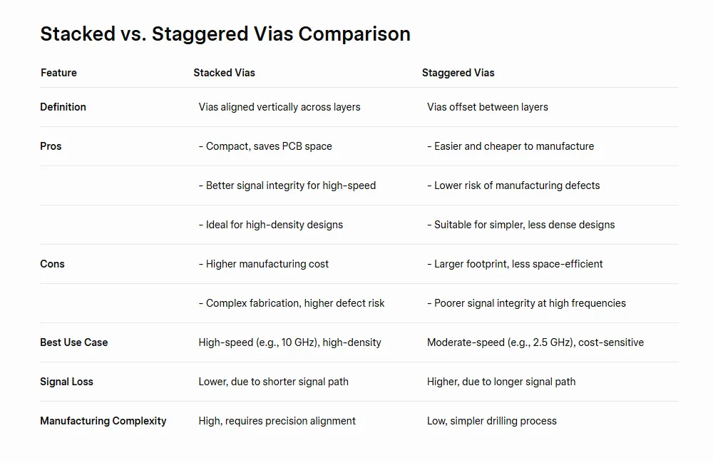
Stacked Vias vs. Staggered Vias: Which Is Right for Your Design?
When deciding between stacked and staggered vias, consider the specific needs of your project. Stacked vias excel in high-density and high-speed applications due to their compact size and superior electrical performance. However, staggered vias may be a better choice for simpler designs or when cost is a primary concern, as they are easier and cheaper to manufacture.
For instance, in a design running at 2.5 GHz with moderate density, staggered vias might suffice with acceptable signal loss. But for a 10 GHz design with tight space constraints, stacked vias are often the only viable option for maintaining stacked via signal integrity.
Conclusion: Elevate Your High-Speed Designs with Stacked Vias
In the realm of high-speed PCB design, stacked vias are a game-changer for achieving top-notch signal integrity. From stacked via impedance control to minimizing signal loss with stacked vias, these structures address critical challenges faced by designers working on cutting-edge electronics. By understanding their benefits, addressing implementation challenges, and following best practices, you can harness the power of stacked vias to create reliable, high-performance PCBs.
Whether you’re designing for telecommunications, consumer electronics, or automotive systems, incorporating stacked vias can make a significant difference in your project’s success. Focus on strategic placement, simulation, and collaboration with your manufacturer to ensure that your designs meet the demands of today’s high-speed world. With stacked vias, you’re not just building a board—you’re building the future of electronics.


