ALLPCB


In the world of printed circuit board (PCB) design, ensuring signal integrity is crucial, especially when it comes to the inner layers of multilayer boards. If you're searching for ways to optimize PCB inner layer signal integrity, achieve impedance control in inner layers, or implement crosstalk reduction in inner layers, you're in the right place. This guide will uncover the secrets of PCB inner layers, offering practical tips and detailed insights to help you design high-performing circuits with minimal signal issues.
Whether you're an experienced engineer or a newcomer to PCB design, understanding how inner layers impact signal quality can make or break your project. In this comprehensive blog, we'll dive deep into the fundamentals of inner layer design, explore techniques for maintaining signal integrity, and provide actionable strategies to tackle common challenges. Let's get started!
What Are PCB Inner Layers and Why Do They Matter for Signal Integrity?
PCB inner layers are the copper layers sandwiched between the outer surfaces of a multilayer board. Unlike the top and bottom layers, which often host components and visible traces, inner layers are hidden within the board's structure. These layers are typically used for routing signals, power distribution, and ground planes in complex designs with high component density.
Signal integrity refers to the ability of a signal to travel through a circuit without distortion, noise, or loss. In multilayer PCBs, inner layers play a critical role in maintaining signal integrity because they often carry high-speed signals or sensitive data lines. Poor design in these layers can lead to issues like signal delay, noise interference, or data errors, especially in high-frequency applications.
For instance, in a 6-layer PCB, the inner layers (layers 2 through 5) might be dedicated to critical signal routing or power delivery. If not designed properly, these layers could introduce unwanted crosstalk or impedance mismatches, degrading the overall performance of the board. Understanding and optimizing inner layer design is, therefore, essential for any high-performance PCB project.
The Importance of PCB Inner Layer Signal Integrity
Maintaining PCB inner layer signal integrity is vital for ensuring that signals remain clear and reliable as they travel through the board. Inner layers are often used for high-speed digital signals or sensitive analog signals, which are particularly prone to distortion. Here are some key reasons why signal integrity matters in these layers:
- High-Speed Signal Transmission: Modern electronics often operate at frequencies above 1 GHz. At these speeds, even small disruptions in the inner layers can cause significant signal loss or timing errors.
- Reduced Noise: Inner layers are shielded from external electromagnetic interference EMI compliance testing, but they can still suffer from internal noise if not designed with proper grounding or spacing.
- Compact Designs: As boards become more compact, inner layers are increasingly used to route dense signal paths, making signal integrity even more challenging to maintain.
By focusing on signal integrity in the inner layers, you can prevent costly redesigns and ensure your PCB performs reliably in real-world conditions.
Key Factors Affecting Signal Integrity in PCB Inner Layers
Several factors influence signal integrity in PCB inner layers. Understanding these elements will help you design boards that minimize signal degradation. Let's explore the most critical aspects below.
1. Impedance Control in Inner Layers
Impedance control in inner layers is a fundamental aspect of maintaining signal integrity. Impedance is the measure of opposition to the flow of alternating current in a circuit, and mismatches can cause signal reflections, leading to data loss or errors. In high-speed designs, controlling impedance ensures that signals travel smoothly without distortion.
In inner layers, impedance is influenced by the trace width, dielectric material thickness, and the proximity to ground or power planes. For example, a typical target impedance for high-speed digital signals might be 50 ohms. If a trace on an inner layer deviates from this value due to inconsistent dielectric spacing or improper trace width (e.g., 5 mils instead of the calculated 7 mils), reflections can occur, degrading signal quality.
Practical Tip: Use simulation tools to calculate the required trace width and spacing for your target impedance. Ensure that the dielectric material between layers (often a prepreg or core material with a specific dielectric constant, such as 4.2 for FR-4) is consistent across the board to avoid variations.
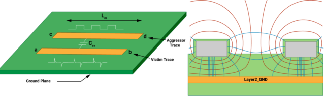
2. Crosstalk Reduction in Inner Layers
Crosstalk reduction in inner layers is another critical concern for signal integrity. Crosstalk occurs when a signal on one trace interferes with a neighboring trace, causing noise or data corruption. In inner layers, where traces are often densely packed, crosstalk can be a significant issue.
To minimize crosstalk, consider the following strategies:
- Increase Trace Spacing: Maintain a spacing of at least 3 times the trace width between adjacent signal traces. For example, if your trace width is 5 mils, aim for a spacing of 15 mils or more.
- Use Ground Planes: Place ground planes on adjacent layers to shield signals and absorb unwanted electromagnetic energy. This is especially effective in inner layers, where signals are surrounded by other conductive layers.
- Route Signals Orthogonally: If possible, route signals on adjacent inner layers in perpendicular directions to reduce coupling. For instance, if layer 2 has horizontal traces, layer 3 should have vertical traces.
By implementing these techniques, you can significantly reduce crosstalk and improve the reliability of your PCB design.
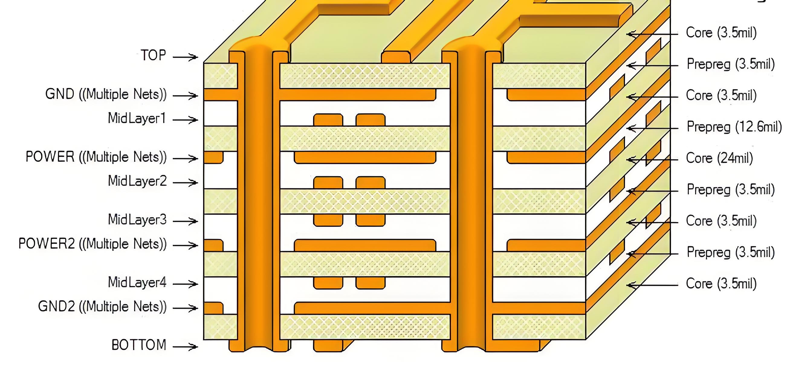
3. Layer Stackup Design
The arrangement of layers in a PCB, known as the stackup, directly impacts signal integrity. A well-designed stackup ensures proper impedance control and minimizes noise in inner layers. For example, in an 8 layer PCB, a common stackup might include signal layers alternating with ground and power planes to provide shielding.
A typical stackup for signal integrity could look like this:
- Layer 1: Top Signal
- Layer 2: Ground Plane
- Layer 3: Inner Signal
- Layer 4: Power Plane
- Layer 5: Power Plane
- Layer 6: Inner Signal
- Layer 7: Ground Plane
- Layer 8: Bottom Signal
This configuration ensures that high-speed signal traces on inner layers (layers 3 and 6) are shielded by adjacent ground or power planes, reducing noise and crosstalk.
Practical Tip: Work with your PCB manufacturer to finalize the stackup early in the design process, as the dielectric thickness and material properties can affect impedance and signal speed.
4. Material Selection for Inner Layers
The choice of dielectric material between inner layers affects signal speed and integrity. Standard FR-4 material, with a dielectric constant (Dk) of about 4.2, is suitable for many designs but may not be ideal for very high-frequency signals (above 5 GHz). For such applications, low-loss materials with a Dk of 3.0 or lower can reduce signal delay and loss.
Additionally, ensure that the copper thickness on inner layers is consistent. Thinner copper (e.g., 0.5 oz) may be used for fine traces, but thicker copper (e.g., 1 oz) is better for power distribution and heat dissipation.
Best Practices for Optimizing PCB Inner Layer Signal Integrity
Now that we've covered the key factors affecting signal integrity, let's look at some best practices for designing inner layers that perform reliably in high-speed and high-frequency applications.
1. Plan Your Routing Strategy
Careful routing of traces on inner layers can prevent many signal integrity issues. Avoid sharp bends in traces, as they can cause signal reflections. Instead, use 45-degree angles or smooth curves for turns. Additionally, keep high-speed signal traces as short as possible to minimize delay and loss.
2. Use Via Stubs Sparingly
Vias connect traces between layers, but long via stubs (unused portions of a via) on inner layers can act as antennas, introducing noise and reflections. If a via stub is unavoidable, consider back-drilling to remove the excess portion, especially for high-speed designs operating above 2 GHz.
3. Simulate and Test Designs
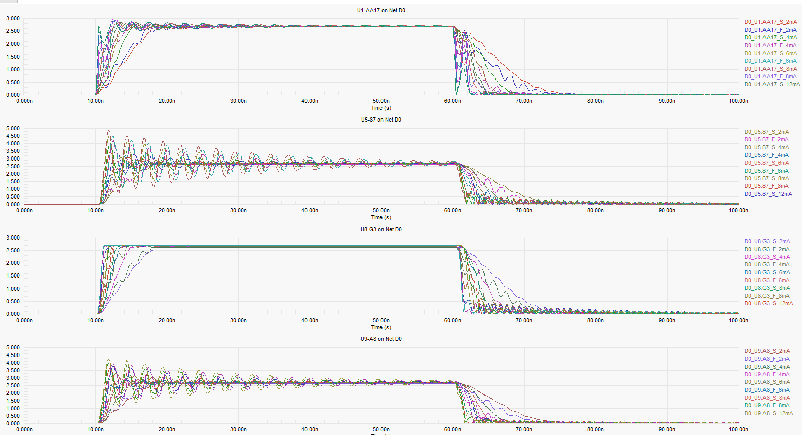
Before finalizing your PCB, use simulation software to analyze signal integrity on inner layers. Tools can model impedance, crosstalk, and signal delay, helping you identify potential issues early. After manufacturing, test the board with oscilloscopes or time-domain reflectometry (TDR) to verify performance against your design goals.
4. Collaborate with Your Manufacturer
Inner layer design often depends on manufacturing capabilities, such as minimum trace width, dielectric thickness, and material availability. Early collaboration with your PCB manufacturer can help you avoid design choices that are difficult or costly to produce, ensuring a smooth transition from design to fabrication.
Common Challenges and Solutions for Inner Layer Signal Integrity
Designing inner layers for optimal signal integrity comes with challenges. Here are some common issues and how to address them:
- Challenge: Impedance Mismatch
Solution: Use controlled impedance design techniques and verify with simulation tools. Ensure consistent dielectric thickness (e.g., 10 mils between layers) and trace width. - Challenge: Crosstalk Between Traces
Solution: Increase spacing between traces and use ground planes for shielding. Route critical signals on separate inner layers if possible. - Challenge: Signal Delay in High-Speed Designs
Solution: Minimize trace length and use low-loss dielectric materials to improve signal speed. For example, a material with a Dk of 3.0 can reduce delay by up to 20% compared to standard FR-4.
Conclusion: Mastering PCB Inner Layer Design for Signal Integrity
Designing PCB inner layers with a focus on signal integrity is a complex but rewarding process. By prioritizing PCB inner layer signal integrity, mastering impedance control in inner layers, and applying techniques for crosstalk reduction in inner layers, you can create boards that perform reliably even in the most demanding applications.
From planning your layer stackup to selecting the right materials and routing strategies, every step in the design process matters. Use the tips and best practices outlined in this guide to tackle common challenges and optimize your PCB for success. With careful attention to detail and the right tools, you can unveil the full potential of your PCB inner layers and achieve outstanding signal integrity.
Remember, a well-designed inner layer is the backbone of any high-performance PCB. Start applying these principles in your next project, and you'll see the difference in both performance and reliability.