 ALLPCB


Stencil printing in a cleanroom environment is a critical process in PCB assembly that can significantly impact the quality and yield of your final product. By controlling contamination and optimizing the setup, manufacturers can achieve consistent solder paste application, reduce defects, and maximize production efficiency. In this comprehensive guide, we’ll explore the best practices for implementing stencil printing in a cleanroom, focusing on contamination control and strategies to boost yield in PCB assembly.
Why Stencil Printing in a Cleanroom Matters for PCB Assembly
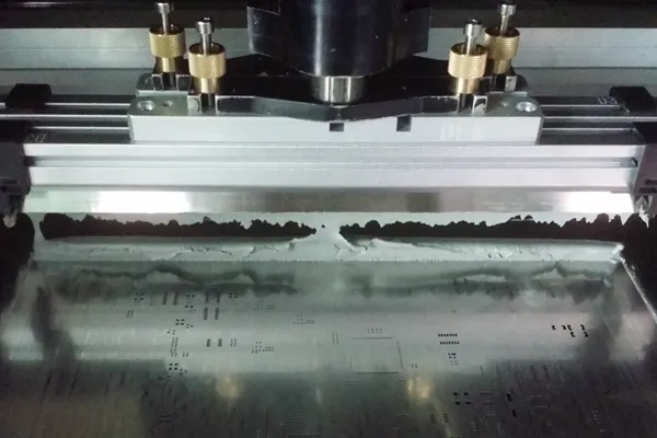
Stencil printing is the first step in surface mount technology (SMT) assembly, where solder paste is applied to the PCB through a stencil. This process determines the accuracy of component placement and the reliability of solder joints. Performing stencil printing in a cleanroom environment is essential because even tiny contaminants like dust, hair, or skin particles can cause defects such as bridging, insufficient solder, or misalignment. These issues lead to rework, increased costs, and lower yields.
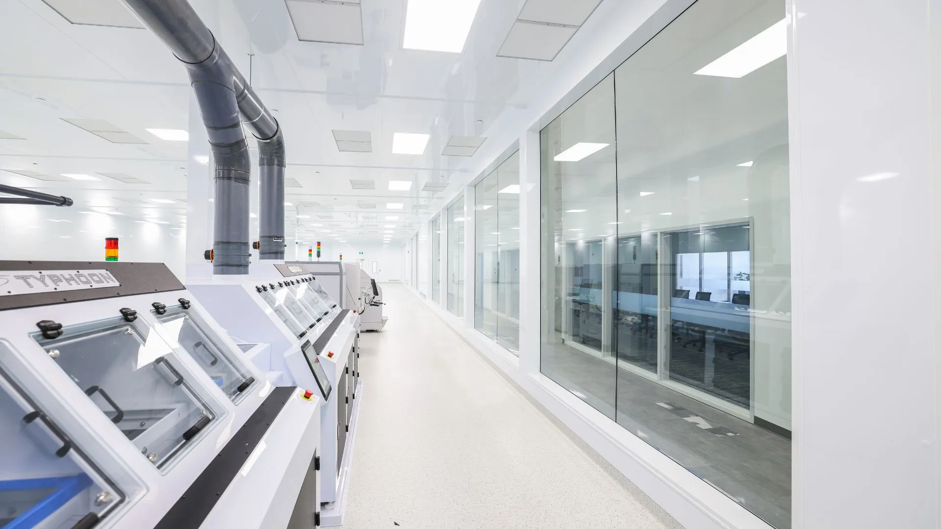
A cleanroom minimizes airborne particles and maintains strict environmental controls, ensuring that the stencil printing process is free from external interferences. For industries like aerospace, medical, and automotive, where reliability is non-negotiable, cleanroom stencil printing is not just a preference—it’s a necessity.
Understanding Cleanroom Standards for PCB Assembly
Cleanrooms are classified based on the number of particles per cubic meter of air, as defined by ISO standards. For PCB assembly, cleanrooms typically range from ISO Class 6 to ISO Class 8, depending on the sensitivity of the components and the precision required. An ISO Class 7 cleanroom, for instance, allows no more than 352,000 particles (0.5 micrometers or larger) per cubic meter, providing a controlled environment suitable for most SMT processes.
Temperature and humidity are also tightly regulated in cleanrooms. A common range for PCB manufacturing is 20-22°C (68-72°F) with a relative humidity of 40-60%. These conditions prevent static electricity buildup, which can attract dust, and ensure that materials like solder paste behave consistently during stencil printing.

Key Challenges of Contamination in Stencil Printing
Contamination during stencil printing can originate from various sources, including airborne particles, human operators, equipment, and even the stencil itself. Here are the primary challenges:
- Airborne Particles: Dust and other microscopic particles can settle on the stencil or PCB, disrupting solder paste application and leading to defects.
- Human Contamination: Skin flakes, hair, or oils from operators can contaminate the workspace if proper protocols are not followed.
- Stencil Residue: Leftover solder paste or debris on the stencil from previous runs can cause inconsistent printing and defects like solder bridging.
- Equipment Issues: Unclean or poorly maintained printers can introduce contaminants or fail to align the stencil properly, affecting print accuracy.
Addressing these challenges requires a combination of strict cleanroom protocols, regular maintenance, and operator training to ensure contamination control at every step of the PCB assembly process.
Best Practices for Contamination Control in a Cleanroom Environment
To minimize contamination during stencil printing in a cleanroom, follow these actionable best practices:
1. Adhere to Cleanroom Protocols
Operators must wear appropriate cleanroom attire, including gloves, hairnets, masks, and full-body suits, to prevent human contamination. Entry and exit procedures, such as air showers, should be mandatory to remove particles from clothing and skin before entering the cleanroom. Additionally, restrict unnecessary movement within the cleanroom to avoid stirring up particles.
2. Use High-Quality Stencils and Materials
Invest in precision-engineered stencils made from stainless steel or nickel, as they offer durability and consistent aperture accuracy. Ensure that stencils are cleaned thoroughly after each use with specialized solvents or ultrasonic cleaners to remove solder paste residues. Store stencils in a dust-free environment to prevent contamination before use.
3. Maintain Equipment Regularly
Stencil printers should be cleaned and calibrated regularly to ensure accurate alignment and pressure during printing. Use lint-free wipes and approved cleaning agents to avoid introducing contaminants. Automated stencil cleaners can also be integrated into the process to reduce manual handling and improve consistency.
4. Control Environmental Factors
Monitor and maintain temperature, humidity, and air filtration systems in the cleanroom. High-efficiency particulate air (HEPA) filters should be used to remove 99.97% of particles as small as 0.3 micrometers from the air. Regularly test the cleanroom environment to ensure it meets the required ISO classification standards.
5. Implement Strict Material Handling
Store solder paste, PCBs, and other materials in sealed containers within the cleanroom to prevent exposure to contaminants. Use anti-static packaging to avoid electrostatic discharge (ESD), which can attract dust and damage sensitive components. Follow first-in, first-out (FIFO) inventory practices to ensure materials are used within their shelf life.
Maximizing Yield Through Optimized Stencil Printing Techniques
Beyond contamination control, optimizing the stencil printing process itself is crucial for maximizing yield in PCB assembly. Yield refers to the percentage of defect-free boards produced in a batch, and even small improvements can lead to significant cost savings. Here are key strategies to enhance yield:
1. Optimize Stencil Design
Stencil design directly impacts solder paste deposition. Aperture size and shape should match the pad layout on the PCB to ensure precise application. For fine-pitch components, consider using step stencils with varying thicknesses to control paste volume in different areas of the board. A typical stencil thickness for standard SMT components is 0.1 to 0.15 mm (4 to 6 mils), but this can be adjusted based on component requirements.
2. Fine-Tune Printing Parameters
Adjust printer settings such as squeegee pressure, speed, and separation speed to achieve uniform solder paste deposits. For example, a squeegee pressure of 0.2 to 0.3 kg/cm2 and a printing speed of 20 to 40 mm/s are common starting points for many setups. Conduct regular print tests and inspect paste deposits using automated optical inspection (AOI) systems to detect and correct issues early.
3. Use High-Quality Solder Paste
Select a solder paste with the right viscosity and particle size for your application. Type 3 or Type 4 solder paste, with particle sizes ranging from 20 to 45 micrometers, is often used for standard SMT components, while Type 5 or smaller may be required for ultra-fine-pitch applications. Ensure the paste is stored at the recommended temperature (typically 2-10°C) and brought to room temperature before use to avoid condensation and contamination.
4. Minimize Downtime with Automation
Automated stencil printers reduce human intervention, improving consistency and reducing the risk of contamination. Features like automatic stencil cleaning and paste dispensing can further streamline the process, minimizing downtime and ensuring repeatable results. Studies suggest that automation can improve first-pass yield by up to 15% in high-volume production environments.
5. Monitor and Analyze Defects
Use statistical process control (SPC) tools to track defects and identify trends in the stencil printing process. Common issues like insufficient solder, bridging, or misalignment can often be traced back to specific parameters or contamination sources. Addressing these root causes promptly helps maintain high yields over time.
Integrating ESD Protection in Cleanroom Stencil Printing
Electrostatic discharge (ESD) is a significant risk in cleanroom environments, as it can damage sensitive components and attract dust particles. Up to one-third of PCB failures are attributed to ESD, making prevention a priority. Use ESD-safe workstations, grounding straps, and anti-static mats during stencil printing. Ensure that all equipment and materials are ESD-compliant, and regularly test grounding systems to maintain effectiveness.
Training and Continuous Improvement
Even with the best equipment and protocols, human error can undermine contamination control and yield. Provide regular training for operators on cleanroom procedures, stencil printing techniques, and ESD prevention. Encourage a culture of continuous improvement by soliciting feedback from the team and implementing small, incremental changes to the process based on real-world performance data.
Conclusion: Achieving Excellence in Cleanroom Stencil Printing
Implementing stencil printing in a cleanroom environment is a powerful way to minimize contamination and maximize yield in PCB assembly. By adhering to strict cleanroom protocols, optimizing stencil design and printing parameters, and integrating automation and ESD protection, manufacturers can achieve consistent, high-quality results. These practices not only reduce defects and rework but also enhance the reliability of the final product, meeting the stringent demands of modern electronics industries.
At ALLPCB, we are committed to supporting your PCB assembly needs with cutting-edge solutions and expertise. Whether you’re looking to refine your stencil printing process or build a cleanroom-ready production line, our team is here to help you achieve unparalleled precision and efficiency.


