 ALLPCB


Are you eager to create your own printed circuit board (PCB) from the comfort of your home? Whether you're a hobbyist, a student, or an aspiring electronics engineer, building a PCB at home is an exciting and rewarding process. In this comprehensive guide, we'll walk you through every step of making a PCB at home, from designing your circuit to etching and assembling the final board. We'll cover the PCB etching process, recommend PCB design software for beginners, highlight essential PCB prototyping tools, and explain how to transfer PCB designs to copper clad boards. Let's dive into the world of DIY PCB prototyping with practical tips and detailed instructions to ensure your success.
Why Build a PCB at Home?
Creating a PCB at home offers several advantages, especially for small projects or learning purposes. It's cost-effective compared to ordering professionally manufactured boards, particularly for one-off designs. It also allows for rapid prototyping, giving you the freedom to test and tweak your ideas quickly. Plus, the hands-on experience of making a PCB at home deepens your understanding of electronics and circuit design. While professional fabrication ensures precision for complex or large-scale projects, DIY methods are perfect for beginners or custom, low-volume boards.
Step 1: Understanding the Basics of PCB Design
Before you start building, it's important to grasp what a PCB is and how it works. A PCB is a board that connects electronic components using conductive traces, usually made of copper, on a non-conductive substrate. These traces replace the mess of wires you'd find in a breadboard setup, making your circuit neat, reliable, and permanent.
For your first project, aim for a simple design, such as a basic LED circuit with resistors. This will help you learn the process without overwhelming complexity. As you gain confidence, you can move on to more intricate designs with microcontrollers or multiple layers.

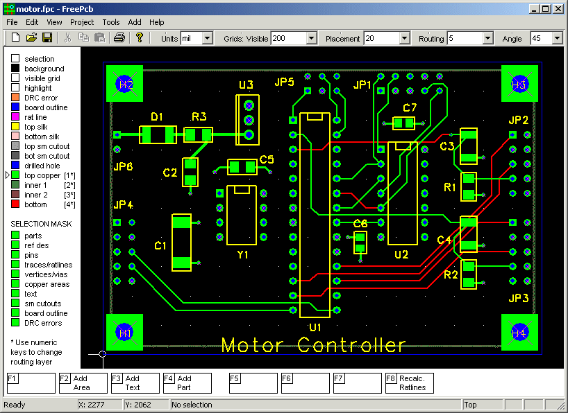
Step 2: Choosing the Right PCB Design Software for Beginners
Designing a PCB starts with creating a digital blueprint of your circuit. Thankfully, there are several user-friendly PCB design software options tailored for beginners. These tools allow you to draw schematics, lay out your board, and generate files needed for fabrication.
Look for free or open-source software with intuitive interfaces and active community support. Popular choices often include programs with drag-and-drop features, libraries of common components, and the ability to export Gerber files, which are standard for PCB manufacturing. Some even offer simulation features to test your circuit virtually before building.
For a beginner, start with software that offers tutorials or built-in templates. Spend time learning the basics, like placing components, routing traces, and setting board dimensions. A typical beginner board might be 5 cm x 5 cm, with trace widths of 0.254 mm (10 mils) for low-current signals. This ensures your design is manageable and fits standard copper clad boards.
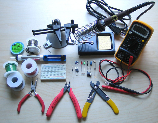
Step 3: Gathering Essential PCB Prototyping Tools and Materials
To bring your design to life, you'll need a set of PCB prototyping tools and materials. Most of these are affordable and can be found online or at local hardware stores. Here's a list of essentials for making a PCB at home:
- Copper Clad Board: This is the base material for your PCB, available in single-sided or double-sided versions. A 10 cm x 15 cm single-sided board is ideal for beginners.
- Etchant Solution: Used to remove unwanted copper during the PCB etching process. Common options include ferric chloride or a safer mix of vinegar, hydrogen peroxide, and salt.
- Laser Printer or Marker: For transferring your design onto the board. A laser printer works best for the toner transfer method.
- Transparency Paper or Glossy Paper: Needed for printing your design if using the toner transfer method.
- Iron or Laminator: To transfer the printed design onto the copper clad board.
- Drill and Bits: For creating holes for through-hole components. A small hand drill with 0.8 mm to 1.2 mm bits works well.
- Safety Gear: Gloves, goggles, and a well-ventilated workspace to handle chemicals safely during etching.
- Basic Tools: Scissors, sandpaper (for cleaning the board), and a container for the etchant.
Having these tools ready will streamline the process and ensure safety while prototyping at home.
Step 4: Designing and Printing Your PCB Layout
Once you've chosen your software, design your circuit by first creating a schematic—a diagram showing how components connect. Then, convert this into a PCB layout, arranging components and routing traces on the board. Keep traces short and avoid sharp angles (use 45-degree turns instead of 90-degree ones) to minimize signal interference. For a beginner project, maintain a trace clearance of at least 0.2 mm to prevent short circuits.
After finalizing your design, print it on transparency or glossy paper using a laser printer. Ensure the print is mirrored if your software doesn’t do this automatically—this ensures the design aligns correctly when transferred to the board. Check that the black areas (representing copper traces) are dark and solid for a clean transfer.
Step 5: Transferring PCB Designs to Copper Clad Boards
Now it's time to transfer your design onto the copper clad board. The toner transfer method is one of the most popular techniques for home prototyping. Here's how to do it:
- Clean the copper clad board with sandpaper or a scrub pad to remove oxidation and ensure a smooth surface. Wipe it with isopropyl alcohol to remove any residue.
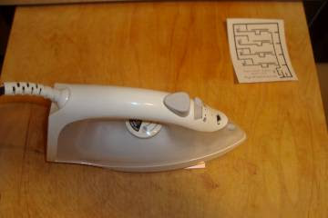
- Place the printed design face down on the copper side of the board. Secure it with tape to prevent shifting.
- Use a hot iron (set to the highest temperature, no steam) or a laminator to heat the paper. Press firmly for 5-10 minutes, ensuring even heat distribution. The toner will melt and adhere to the copper.
- Let the board cool, then soak it in water for 10-15 minutes to soften the paper. Gently peel or rub off the paper, leaving the toner design on the copper.
- Inspect the board for any broken traces. If needed, use a permanent marker to touch up gaps or weak areas.
This step is critical for a successful PCB etching process, as any flaws in the transfer can lead to incomplete traces or shorts.
Step 6: The PCB Etching Process at Home
The PCB etching process removes unwanted copper from the board, leaving only the traces protected by the toner. Follow these steps carefully to achieve clean results:
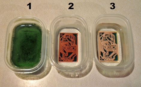
- Prepare your etchant solution in a non-metallic container. If using ferric chloride, follow the manufacturer's instructions (typically a 1:3 ratio with water). For a safer alternative, mix equal parts vinegar and hydrogen peroxide, then add a teaspoon of salt per cup of solution.
- Wear gloves and goggles, and work in a well-ventilated area. Place the board in the etchant, copper side up, and agitate the container gently to speed up the process.
- Check the board every 5-10 minutes. Etching usually takes 20-40 minutes, depending on the solution and temperature. The exposed copper will dissolve, revealing the substrate underneath.
- Once the unwanted copper is gone, remove the board and rinse it thoroughly with water to stop the etching. Dispose of the used etchant safely according to local regulations.
- Use acetone or alcohol to remove the toner, revealing the copper traces underneath.
Be patient during etching—rushing can lead to under-etched or over-etched boards. If traces are too thin (e.g., below 0.1 mm), you risk breakage during use, especially for currents above 1A.
Step 7: Drilling Holes and Cleaning the Board
After etching, drill holes for through-hole components using a small hand drill or a drill press. Match the drill bit size to your component leads—0.8 mm bits work for most resistors and capacitors. Drill slowly to avoid damaging the board or breaking the bit.
Once drilling is complete, clean the board again with sandpaper to remove burrs around the holes. This ensures smooth insertion of components and better soldering results.
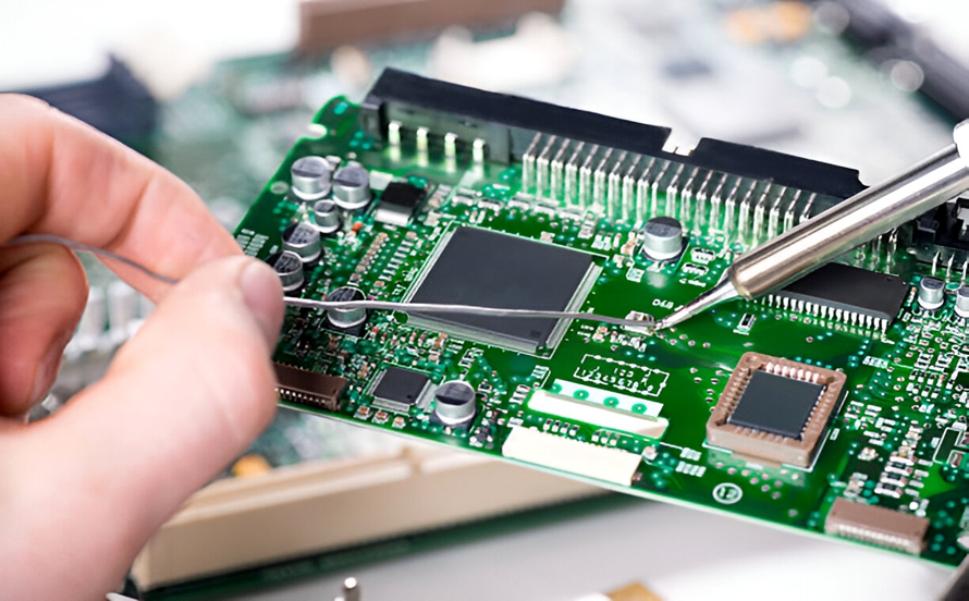
Step 8: Soldering Components and Testing
Now, populate your board by inserting components into the drilled holes. Double-check their placement against your schematic to avoid errors. Heat your soldering iron to around 300°C (572°F) for general-purpose soldering. Apply solder to the pads, ensuring a shiny, cone-shaped joint without excess solder (which can cause shorts).
After soldering, inspect the board for cold joints or bridges between traces. Use a multimeter to test continuity and verify that connections match your design. Power up the circuit with a low voltage (e.g., 5V for most beginner projects) to check functionality. If an LED circuit is your first project, ensure the LED lights up at the expected current, typically 20 mA with a suitable resistor.
Step 9: Troubleshooting Common Issues in DIY PCB Prototyping
Building a PCB at home can come with challenges. Here are some common issues and how to fix them:
- Incomplete Toner Transfer: If traces don't transfer fully, ensure the board is clean and apply more heat or pressure during transfer.
- Over-Etching: If traces are too thin or broken, reduce etching time or dilute the solution. Check the board frequently during the process.
- Short Circuits: Inspect for solder bridges or toner smudges before etching. Use a multimeter to identify and fix shorts.
- Component Misalignment: Verify component placement before soldering. Desoldering can be tricky and may damage the board.
Patience and attention to detail will help you avoid most of these pitfalls.
Step 10: Scaling Up from Home Prototyping to Professional Boards
Once you're comfortable making a PCB at home, you might want to explore professional manufacturing for more complex designs. Professional services offer higher precision, multilayer boards, and finer trace widths (down to 0.1 mm or less), which are hard to achieve with DIY methods. They also handle high-frequency designs where impedance control (e.g., 50 ohms for RF circuits) is critical.
Start by exporting Gerber files from your design software—these files include all layers and drill information needed for production. Partnering with a reliable fabrication service can save time and ensure quality for larger projects or final products.
Tips for Success in Home PCB Prototyping
To wrap up, here are some practical tips to make your DIY PCB journey smoother:
- Start small with simple circuits to build skills before tackling complex designs.
- Always prioritize safety when handling chemicals for the PCB etching process. Use protective gear and work in a ventilated space.
- Keep a notebook or digital log of your designs, mistakes, and solutions to learn from each project.
- Invest in quality PCB prototyping tools over time, as they improve accuracy and efficiency.
- Practice transferring PCB designs to copper clad boards multiple times on scrap pieces to perfect the technique.
Conclusion: Start Building Your First PCB Today
Building your first PCB at home is a fantastic way to bring your electronic ideas to life. By following this step-by-step guide, you've learned how to design a circuit using PCB design software for beginners, gather the right PCB prototyping tools, execute the PCB etching process, and successfully transfer PCB designs to copper clad boards. Each step, from design to soldering, builds your skills and confidence as a maker.
With practice, you'll master making a PCB at home and may even transition to professional fabrication for advanced projects. Grab your tools, start with a simple design, and enjoy the satisfaction of creating a functional circuit board from scratch. The world of electronics prototyping awaits!


