 ALLPCB


If you're looking for effective ways to fix a damaged printed circuit board (PCB), you've come to the right place. Repairing and reworking PCBs can save time, reduce costs, and extend the life of electronic devices. In this guide, we’ll dive into advanced PCB repair techniques and PCB rework methods to address issues like broken traces, damaged pads, and other common problems. Whether you're dealing with a cracked board or a faulty connection, these methods will help you restore functionality with precision.
Below, we’ll explore detailed steps, tools, and best practices for damaged PCB repair, including PCB trace repair and PCB pad repair. Let’s get started with actionable insights to tackle even the most challenging repairs.
Why PCB Repair and Rework Matter
PCBs are the backbone of modern electronics, connecting components like resistors, capacitors, and integrated circuits (ICs) to ensure devices function properly. However, factors like physical stress, overheating, or moisture can lead to damage. Throwing away a damaged board isn’t always the best option—repairing it can be more cost-effective, especially for complex or custom designs.
Mastering PCB repair techniques and PCB rework methods allows engineers and technicians to salvage boards, reduce waste, and maintain project timelines. With the right skills, even severe issues like broken traces or torn pads can be fixed, restoring a board to full operation.
Common Causes of PCB Damage
Before diving into repair methods, it’s important to understand what causes PCB damage. Identifying the root cause can help prevent future issues and guide the repair process. Here are some common reasons for PCB failure:
- Physical Stress: Dropping a device or applying excessive force during assembly can crack the board or break traces.
- Thermal Damage: Overheating from high-power components or poor heat dissipation can burn traces or components, often exceeding safe temperatures of 85°C for standard FR-4 boards.
- Moisture and Corrosion: Exposure to humidity can corrode copper traces, leading to open circuits or short circuits.
- Component Failure: A failed component, like a burnt capacitor, can damage nearby traces or pads, disrupting signal integrity.
- Manufacturing Defects: Issues like poor soldering or misaligned components during production can create weak points that fail over time.
Understanding these causes helps in diagnosing issues accurately during damaged PCB repair. Now, let’s look at the tools and techniques needed for effective repairs.
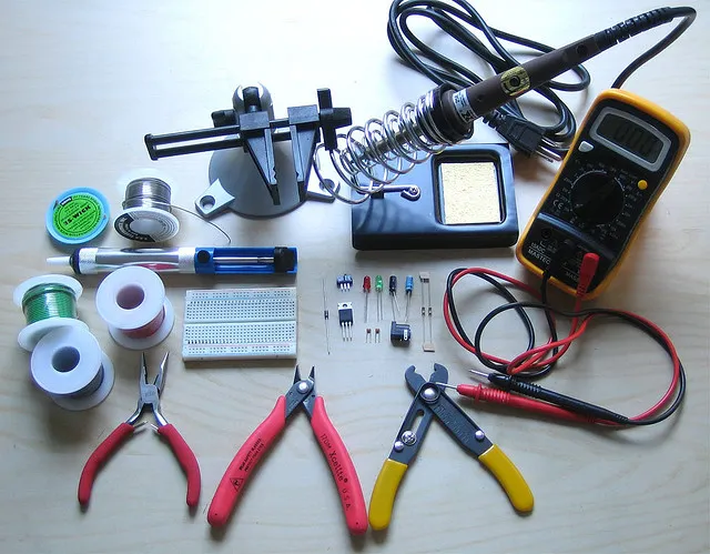
Essential Tools for PCB Repair and Rework
Having the right tools is critical for precise and safe PCB repair. Here’s a list of must-have equipment for PCB rework methods and repairs:
- Soldering Iron: A fine-tip soldering iron (15-30W) for precise work on small components and traces.
- Desoldering Tools: Desoldering pumps or wick to remove old solder without damaging pads.
- Hot Air Rework Station: For removing and replacing surface-mount components with controlled heat (typical range: 100-480°C).
- Multimeter: To test continuity, voltage, and resistance, ensuring traces and components function correctly (e.g., checking for 0 ohms on a good trace).
- Magnifying Glass or Microscope: For inspecting tiny traces and pads, often at 10x-40x magnification.
- Conductive Epoxy or Wire: For repairing broken traces during PCB trace repair.
- Replacement Pads and Components: To restore damaged areas in PCB pad repair.
- Cleaning Supplies: Isopropyl alcohol (90% or higher) and brushes to clean flux residue or contaminants.
With these tools in hand, you’re ready to tackle advanced PCB repair techniques. Let’s move on to specific methods for common issues.
Related Reading: PCB Rework Station for Beginners: A Simple Guide to Component Replacement
Advanced PCB Repair Techniques
Repairing a damaged PCB requires patience and precision. Below are step-by-step methods for addressing common issues like broken traces and damaged pads.
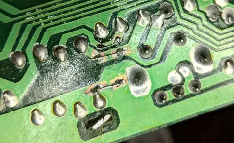
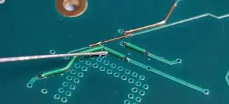
1. PCB Trace Repair: Restoring Broken Connections
Traces are thin copper lines on a PCB that carry electrical signals. When they break due to physical damage or corrosion, the circuit becomes incomplete. Here’s how to perform PCB trace repair:
- Inspect the Damage: Use a magnifying glass to locate the broken trace. Look for visible cracks or burnt areas.
- Clean the Area: Remove dirt or oxidation using isopropyl alcohol and a small brush. Ensure the area is dry before proceeding.
- Expose Copper (if needed): If the trace is covered by solder mask, gently scrape it away with a fine blade to expose the copper underneath.
- Bridge the Gap: For small breaks (less than 1 mm), apply a thin layer of conductive epoxy or solder to reconnect the trace. For larger gaps, solder a thin jumper wire (e.g., 30 AWG) across the break.
- Test Continuity: Use a multimeter to confirm the trace now shows 0 ohms resistance, indicating a complete connection.
- Protect the Repair: Apply a layer of conformal coating or UV-curable solder mask to insulate the repaired area and prevent future damage.
This method ensures signal integrity is restored, often maintaining impedance close to the original design (e.g., 50 ohms for standard high-frequency traces).
Related Reading: Understanding IPC Standards for Rework and Repair of Electronic Assemblies
2. PCB Pad Repair: Fixing Torn or Lifted Pads
Pads are the small copper areas where components are soldered. They can lift or tear due to excessive heat or mechanical stress. Here’s a detailed approach to PCB pad repair:
- Assess the Damage: Check if the pad is completely torn off or just lifted. If the underlying trace is intact, repair is easier.
- Clean the Area: Use isopropyl alcohol to remove debris and old solder from the damaged pad area.
- Prepare a Replacement Pad: If the pad is missing, use a copper foil or a pre-made replacement pad cut to size. Secure it with adhesive if needed.
- Reconnect the Pad: Solder the replacement pad to the trace, ensuring a strong electrical connection. Keep soldering time under 3 seconds per joint to avoid heat damage.
- Attach the Component: Solder the component lead to the new pad, verifying alignment and connection with a multimeter.
- Secure the Repair: Apply a small amount of epoxy or conformal coating around the pad for added durability.
This technique is crucial for surface-mount and through-hole components, ensuring reliable connections even under thermal cycles (e.g., 25°C to 85°C operating range).
3. Component Replacement in PCB Rework
Sometimes, damaged components cause PCB issues. Replacing them is a key part of PCB rework methods. Follow these steps for surface-mount device (SMD) replacement:
- Remove the Faulty Component: Use a hot air rework station to heat the solder joints (around 300°C for lead-free solder). Gently lift the component with tweezers once the solder melts.
- Clean the Pads: Remove excess solder using desoldering wick and clean the area with alcohol.
- Apply Fresh Solder: Add a thin layer of solder paste or flux to the pads to prepare for the new component.
- Place the New Component: Align the replacement component carefully and use the hot air station to reflow the solder, securing it in place.
- Inspect the Joints: Check for cold solder joints or misalignment under magnification. Reflow if necessary.
- Test the Circuit: Power on the board and use a multimeter to verify voltage levels and signal paths (e.g., 3.3V for logic circuits).
This method is ideal for fixing issues caused by failed ICs or capacitors, common in high-density boards.
Best Practices for Damaged PCB Repair
To ensure long-lasting repairs and prevent further damage, follow these best practices during damaged PCB repair:
- Work in a Static-Free Environment: Use an anti-static wrist strap and mat to prevent electrostatic discharge (ESD), which can damage sensitive components (typical ESD threshold: 100V).
- Control Heat Exposure: Avoid overheating traces or components by limiting soldering iron contact to 2-3 seconds per joint and using heat sinks if needed.
- Document the Repair: Take photos or notes of the board’s layout before starting repairs to avoid misplacement of components or wires.
- Test Incrementally: After each repair step, test the board to ensure the fix didn’t introduce new issues, such as shorts or signal noise.
- Use Quality Materials: Opt for high-grade solder (e.g., 63/37 tin-lead) and components to ensure reliability over time.
These practices minimize risks and improve the success rate of PCB repair techniques.
Challenges in PCB Rework and How to Overcome Them
Even with advanced skills, PCB rework can present challenges. Here are common issues and solutions:
- Multilayer Boards: Damage in internal layers is hard to access. Use X-ray inspection if available, or focus on external connections and vias.
- Small Components: Tiny SMD parts (e.g., 0402 size, 1mm x 0.5mm) are difficult to handle. Use precision tweezers and a steady hand under high magnification.
- Heat Damage Risk: Excessive heat can delaminate the board. Work in short bursts and monitor temperature closely with a thermal probe.
- Complex Circuits: High-speed designs (e.g., signal speeds above 1 GHz) require precise impedance matching. Use conductive materials that match the original trace properties as closely as possible.
Patience and the right tools can help overcome these hurdles, ensuring successful PCB rework methods.
Preventing Future PCB Damage
While repairs are valuable, preventing damage is even better. Here are tips to protect PCBs after rework:
- Apply Conformal Coating: Use a protective layer to shield against moisture and dust after completing repairs.
- Improve Heat Management: Add heat sinks or ventilation to prevent thermal stress on components operating above 70°C.
- Handle with Care: Store and transport PCBs in protective cases to avoid physical stress or cracks.
- Regular Maintenance: Inspect boards periodically for signs of wear, corrosion, or loose connections, addressing issues early.
These steps extend the lifespan of repaired boards and reduce the need for future damaged PCB repair.
Conclusion: Mastering PCB Repair and Rework
Repairing and reworking damaged PCBs is a valuable skill for anyone working with electronics. By using advanced PCB repair techniques like PCB trace repair and PCB pad repair, you can salvage boards that might otherwise be discarded. With the right tools, methods, and best practices, even complex issues can be resolved, restoring full functionality to your circuits.
Whether you're fixing a broken trace with a jumper wire or replacing a torn pad with copper foil, precision and patience are key. By following the detailed steps and tips outlined in this guide, you’ll be well-equipped to handle damaged PCB repair challenges and apply effective PCB rework methods. Keep learning and practicing, and you’ll master the art of PCB restoration in no time.


