 ALLPCB


In high-speed PCB design, maintaining signal integrity is critical for ensuring reliable performance. One key factor that directly affects signal integrity is the maximum line width of PCB traces, often referred to as trace width. But how does trace width impact signal integrity in high-speed PCBs? Simply put, the width of a trace influences impedance, signal reflection, and overall signal quality. Incorrect trace widths can lead to issues like crosstalk, signal distortion, and data loss, especially in high-frequency applications.
In this blog, we’ll dive deep into the relationship between maximum line width and signal integrity, exploring concepts like impedance control trace width, signal reflection trace width, and controlled impedance PCB design. Whether you’re an engineer working on high-speed PCB layout or simply looking to understand these principles, this guide will provide actionable insights to help you optimize your designs for better performance.
What Is Signal Integrity in High-Speed PCBs?
Signal integrity refers to the quality of an electrical signal as it travels through a PCB. In high-speed designs, where signals switch at frequencies of hundreds of megahertz or even gigahertz, maintaining signal integrity becomes challenging. Poor signal integrity can result in errors, delays, or complete failure of the system. Factors like noise, crosstalk, and signal reflection can degrade the signal, and trace width plays a significant role in managing these issues.
In high-speed PCB layouts, signals must travel without distortion to ensure data is transmitted accurately. For example, in a 5G communication board operating at 3 GHz, even a slight mismatch in trace width can cause impedance variations, leading to reflections that disrupt the signal. Understanding how maximum line width impacts signal integrity is the first step in designing reliable high-speed circuits.
Why Trace Width Matters for Signal Integrity
The width of a PCB trace determines its electrical characteristics, particularly its impedance. Impedance is the resistance to the flow of an alternating current signal, and in high-speed designs, controlling impedance is essential for signal integrity. A trace that is too wide or too narrow can cause an impedance mismatch, leading to signal reflections and loss of data integrity.
For instance, a wider trace typically has lower impedance because it offers less resistance to the signal. Conversely, a narrower trace increases impedance. If the trace width doesn’t match the required impedance for the circuit (often 50 ohms for many high-speed applications), the signal can reflect back along the trace, causing interference. This is a critical concern in high-speed PCB layouts where timing and signal clarity are paramount.
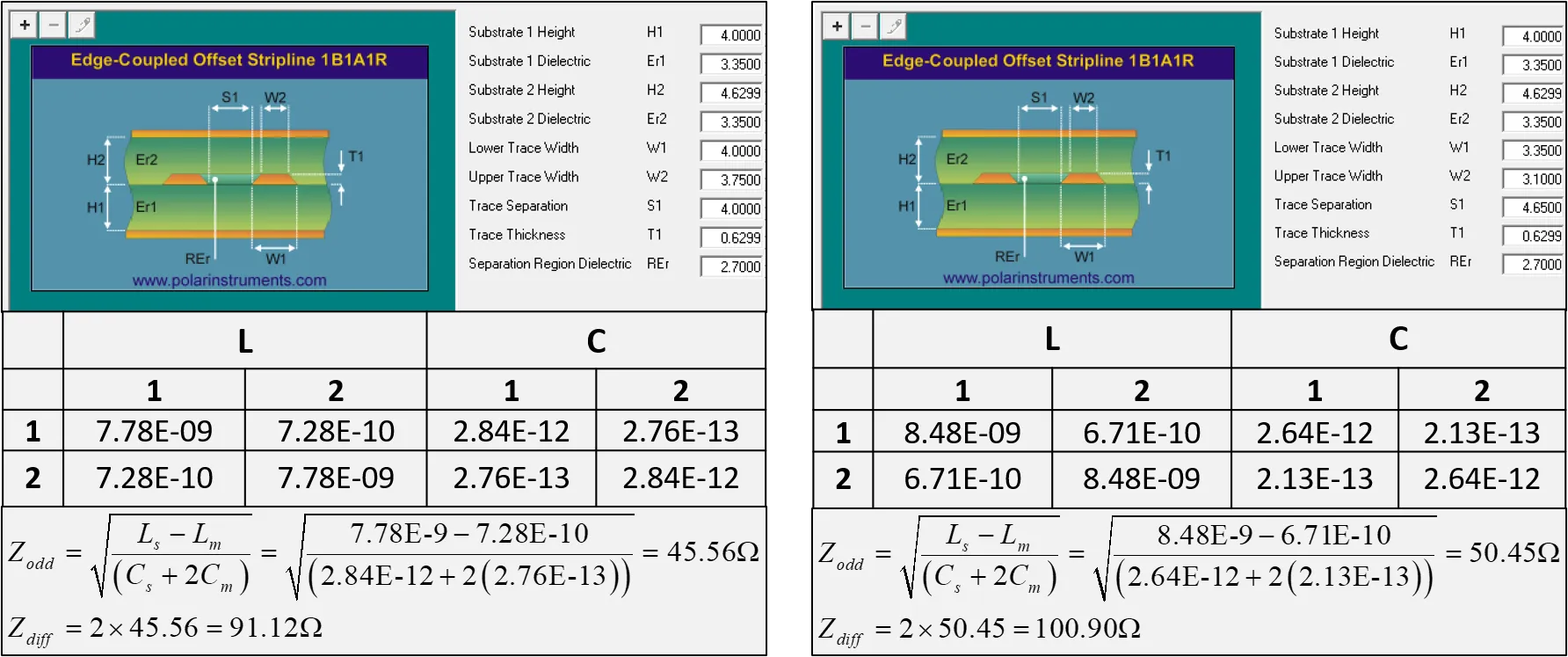
Impedance Control Trace Width: Striking the Right Balance
Controlled impedance PCB design is a technique used to maintain a consistent impedance value along a trace. This is especially important in high-speed designs where signals must travel without significant distortion. The trace width is a primary factor in achieving controlled impedance, alongside other elements like trace thickness, dielectric material, and spacing from the ground plane.
To calculate the appropriate trace width for impedance control, designers often use formulas or simulation tools. For a microstrip trace (a common configuration in PCBs), the impedance can be approximated using the following relationship:
- Impedance (Z) ∝ 1 / (trace width)
- Impedance also depends on the height of the dielectric layer and the dielectric constant of the material.
For example, a 50-ohm impedance might require a trace width of 6 mils (0.006 inches) on a standard FR-4 material with a dielectric height of 10 mils. If the trace width increases to 10 mils, the impedance could drop to around 40 ohms, causing a mismatch. Such mismatches are a common cause of signal reflection in high-speed PCB layouts.
By carefully selecting the maximum line width, designers can achieve the target impedance, minimizing signal reflection trace width issues. This process often involves collaboration with fabrication teams to ensure the chosen width is manufacturable and consistent across the board.
Signal Reflection Trace Width: Avoiding Reflections in High-Speed Designs
Signal reflection occurs when a signal encounters a change in impedance along its path, causing part of the signal to bounce back toward the source. In high-speed PCB layouts, reflections can distort the signal, leading to errors in data transmission. Trace width plays a direct role in this phenomenon because it affects impedance.
For instance, if a trace narrows suddenly in a confined area of the PCB, the impedance increases at that point, causing a reflection. Similarly, a trace that is too wide may lower the impedance excessively, leading to a mismatch with connected components. Research shows that even a 10% change in trace width can result in measurable reflections at frequencies above 1 GHz.
To minimize signal reflection trace width issues, maintain consistent trace widths wherever possible. If a width change is unavoidable due to layout constraints, use gradual transitions or tapers to reduce abrupt impedance shifts. Additionally, routing high-speed signals away from areas with frequent width changes can help preserve signal integrity.
High-Speed PCB Layout: Best Practices for Trace Width Selection
Designing a high-speed PCB layout requires careful consideration of trace width to ensure signal integrity. Here are some best practices for selecting the maximum line width in your designs:
- Match Impedance Requirements: Use simulation tools or impedance calculators to determine the trace width needed for your target impedance. For example, a 100-ohm differential pair might require traces of 5 mils each with a specific spacing.
- Consider Frequency: Higher frequencies are more sensitive to impedance mismatches. For signals above 500 MHz, even small variations in trace width can impact performance.
- Account for Manufacturing Tolerances: Fabrication processes may introduce slight variations in trace width, typically ±10%. Design with these tolerances in mind to avoid unexpected impedance shifts.
- Route with Consistency: Avoid sudden changes in trace width. If a change is necessary, use a gradual taper over a length of at least 10 times the width change to minimize reflections.
- Use Ground Planes: A solid ground plane beneath high-speed traces helps maintain consistent impedance and reduces noise, complementing proper trace width selection.
By following these guidelines, you can optimize your high-speed PCB layout for better signal integrity and performance. These practices are especially important in applications like USB 3.0, HDMI, or DDR memory interfaces, where signal timing is critical.
Challenges of Maximum Line Width in Controlled Impedance PCB Design
While wider traces can reduce resistance and heat dissipation, using the maximum line width isn’t always ideal for controlled impedance PCB design. Wider traces lower impedance, which may not align with the circuit’s requirements. For example, a trace width of 20 mils might result in an impedance of 30 ohms, which is too low for a standard 50-ohm system, leading to signal integrity issues.
Additionally, wider traces take up more space on the PCB, which can be a problem in compact designs. This often forces designers to balance impedance control with layout constraints. In some cases, using narrower traces with higher impedance may be necessary, but this increases resistance and the risk of overheating in high-current applications.
Another challenge is maintaining uniform trace width across the board during manufacturing. Etching processes can introduce variations, especially for very wide or very narrow traces. Working closely with your fabrication partner ensures that the maximum line width you specify is achievable and consistent, preserving signal integrity.
The Role of Materials and Stack-Up in Trace Width Selection
Beyond trace width, the materials used in a PCB and its layer stack-up also influence signal integrity. The dielectric constant (Dk) of the PCB material affects how signals propagate through the traces. For instance, FR-4, a common PCB material, has a Dk of around 4.2, while high-speed materials like Rogers 4350 have a lower Dk of 3.5, allowing for different trace width calculations to achieve the same impedance.
The stack-up, or arrangement of layers in the PCB, also plays a role. A trace on an outer layer (microstrip) will have a different impedance compared to an inner layer trace (stripline) even if the width is the same. Designers must account for these factors when determining the maximum line width for high-speed signals.
For example, a 6-mil trace on a microstrip layer might achieve 50 ohms with a 10-mil dielectric height, while the same width on a stripline layer might require adjustments due to the surrounding ground planes. Understanding the interplay between trace width, materials, and stack-up is essential for maintaining signal integrity in high-speed PCB layouts.
Tools and Simulations for Optimizing Signal Integrity PCB Trace Width
Modern PCB design tools offer powerful simulation features to help engineers optimize trace width for signal integrity. These tools can model impedance, predict signal reflection, and analyze crosstalk based on trace dimensions and material properties. Some common approaches include:
- Field Solvers: These calculate the exact impedance of a trace based on its width, thickness, and surrounding environment.
- Time-Domain Reflectometry (TDR): This technique measures reflections along a trace to identify impedance mismatches caused by incorrect widths.
- Signal Integrity Analysis: Simulates how signals behave under different trace width configurations, helping to fine-tune the design.
Using these tools, engineers can experiment with different trace widths before fabrication, reducing the risk of signal integrity issues. For instance, simulating a 10-mil trace versus a 6-mil trace can reveal how each affects signal timing at 2 GHz, allowing for informed design decisions.
Conclusion: Balancing Maximum Line Width and Signal Integrity
The maximum line width of PCB traces has a profound impact on signal integrity in high-speed designs. By carefully selecting trace widths based on impedance control requirements, designers can minimize signal reflection, reduce crosstalk, and ensure reliable performance. Key considerations include matching impedance targets, accounting for manufacturing tolerances, and using consistent routing practices in high-speed PCB layouts.
Whether you’re working on a cutting-edge communication system or a high-performance computing board, understanding the relationship between signal integrity PCB trace width and other design factors is essential. With the right tools, materials, and design strategies, you can optimize your PCB for maximum signal quality and efficiency.


