 ALLPCB


If you're designing or manufacturing a printed circuit board (PCB), avoiding solder mask errors is critical to ensuring a reliable and functional product. Common solder mask mistakes, such as improper clearances, misaligned layers, or incomplete via tenting, can lead to issues like solder bridges and electrical shorts. In this comprehensive guide, we'll explore the top solder mask errors, PCB design mistakes, and practical tips to avoid solder bridges and solder resist problems, helping you achieve a flawless PCB design and manufacturing process.
What Is a Solder Mask and Why Is It Important?
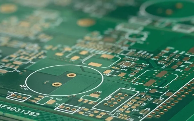
A solder mask, also known as solder resist, is a thin protective layer of polymer applied to the surface of a PCB. Its primary purpose is to shield the copper traces from oxidation, prevent accidental solder bridges during assembly, and provide electrical insulation between conductive paths. Without a properly applied solder mask, your PCB risks short circuits, corrosion, and assembly errors that could render the board unusable.
However, even a small error in the solder mask design or application can lead to significant problems. Let's dive into the most common solder mask errors and PCB design mistakes to avoid, ensuring your boards are both reliable and cost-effective to produce.
Top Solder Mask Errors to Avoid
Designing and applying a solder mask requires precision. Below are some of the most frequent solder mask errors that PCB designers and manufacturers encounter, along with tips to prevent them.
1. Inadequate Clearance Around SMD Pads
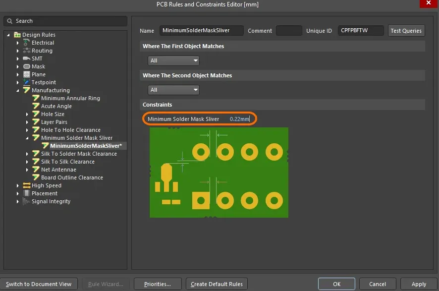
One of the most common solder mask errors is insufficient clearance between the solder mask and surface-mount device (SMD) pads. If the solder mask is too close to the pad, it can interfere with the soldering process, leading to poor connections or uneven solder distribution. Ideally, the solder mask should have a clearance of at least 0.1 mm (4 mils) around SMD pads to allow for proper solder flow and alignment during assembly.
Tip to Avoid: Always review your design files to ensure proper clearance. Use design rule checks (DRC) in your PCB design software to automatically flag areas where the solder mask might be too close to pads.
2. Incomplete Via Tenting
Vias are small holes in a PCB that connect different layers of the board. Tenting refers to covering these vias with a solder mask to prevent solder from flowing into them during assembly. Incomplete via tenting can lead to solder wicking, where molten solder enters the via and causes shorts or weak connections elsewhere on the board.
Tip to Avoid: Specify in your design whether vias should be tented, plugged, or left open based on their purpose. For most designs, tenting vias with a solder mask on both sides is recommended unless they are used for test points or need to remain exposed.
3. Solder Mask Misalignment
Solder mask misalignment happens when the mask layer is not properly aligned with the copper traces and pads during manufacturing. This can expose areas of copper that should be protected, leading to oxidation or accidental solder bridges. Misalignment often occurs due to errors in design files or manufacturing tolerances not being accounted for.
Tip to Avoid: Include a solder mask expansion of at least 0.05 mm (2 mils) beyond the copper edges in your design to account for minor misalignments. Additionally, work with your manufacturing partner to confirm their alignment capabilities and adjust your design accordingly.
4. Overlapping Silkscreen and Solder Mask
The silkscreen layer, which contains text and symbols for component identification, should not overlap with the solder mask openings. If it does, the silkscreen ink can interfere with soldering or become illegible, causing confusion during assembly or testing.
Tip to Avoid: Ensure there is at least a 0.2 mm (8 mils) gap between silkscreen markings and solder mask openings. Use your design software's DRC tools to catch any overlaps before finalizing your files.
5. Incorrect Solder Mask Thickness
The thickness of the solder mask layer is crucial for effective protection. If it's too thin, it may not provide adequate insulation or protection against environmental factors. If it's too thick, it can interfere with component placement or soldering. A typical solder mask thickness ranges from 0.8 to 1.2 mils (0.02 to 0.03 mm), depending on the PCB's application.
Tip to Avoid: Specify the desired solder mask thickness in your design documentation and confirm with your manufacturer that they can meet this requirement. Regularly test prototypes to ensure the applied thickness meets your specifications.
6. Ignoring Solder Mask Color Impact
While solder mask color might seem like a purely aesthetic choice, it can impact inspection and performance. For example, green is the most common color because it provides good contrast for visual inspection. Using less common colors like white or black can make it harder to spot defects or may affect heat dissipation in high-power applications.
Tip to Avoid: Stick to standard colors like green unless there’s a specific reason for a different choice. If you opt for a non-standard color, ensure it won’t hinder inspection processes or thermal performance.
PCB Design Mistakes That Lead to Solder Resist Problems
Beyond specific solder mask errors, broader PCB design mistakes can also contribute to solder resist problems. Addressing these issues early in the design phase can save time and reduce costs during manufacturing.
1. Poor Component Placement
Placing components too close together can make it difficult to apply the solder mask evenly, increasing the risk of solder bridges. This is especially problematic in high-density designs where space is limited.
Tip to Avoid: Maintain a minimum spacing of 0.3 mm (12 mils) between components and pads to allow for proper solder mask application and soldering. Use design software to simulate assembly and identify potential spacing issues.
2. Insufficient Pad Sizes
Small or uneven pad sizes can cause solder skips, where solder fails to adhere properly during assembly. This often happens when pads are not designed to accommodate the component's footprint or the soldering process used (e.g., wave soldering with a specific wave height).
Tip to Avoid: Follow the recommended pad sizes for each component as specified in their datasheets. For SMD components, ensure pads are at least 0.2 mm (8 mils) larger than the component’s contact area to account for manufacturing tolerances.
3. Neglecting Thermal Considerations
High-power components generate heat, which can degrade the solder mask over time if not accounted for in the design. Cracked or peeling solder mask layers can expose copper traces, leading to corrosion or shorts.
Tip to Avoid: Use thermal relief pads for components that dissipate significant heat (e.g., power ICs with dissipation above 1W). Additionally, consider high-temperature-resistant solder mask materials for boards operating in harsh environments.
How to Avoid Solder Bridges in PCB Assembly
Solder bridges occur when excess solder connects two adjacent pads or traces, creating an unintended electrical connection. This is a common issue during PCB assembly, often linked to solder mask errors or design flaws. Here are actionable steps to avoid solder bridges.
1. Optimize Solder Mask Openings
Solder mask openings that are too large can allow excess solder to flow onto adjacent areas, increasing the risk of bridges. Conversely, openings that are too small can prevent proper solder adhesion.
Tip to Avoid: Design solder mask openings to be slightly smaller than the pad size, typically by 0.1 mm (4 mils) on each side, to control solder flow while ensuring good contact.
2. Use Proper Soldering Techniques
During assembly, using the wrong soldering temperature or applying too much solder paste can lead to bridges. For example, a reflow oven temperature that exceeds the recommended profile (often around 240–260°C for lead-free solder) can cause solder to spread excessively.
Tip to Avoid: Follow the solder paste manufacturer’s recommended reflow profile and use stencil designs with appropriate aperture sizes to control the amount of paste applied.
3. Inspect and Test Regularly
Even with a perfect design, manufacturing variations can lead to solder bridges. Automated optical inspection (AOI) systems can detect bridges and other defects with a resolution down to 0.025 mm (1 mil), catching issues before they cause failures.
Tip to Avoid: Incorporate AOI or X-ray inspection into your quality control process, especially for high-density boards with fine-pitch components (below 0.5 mm pitch).
Best Practices for Solder Mask Design and Application
To minimize solder mask errors and solder resist problems, follow these best practices during the design and manufacturing stages.
- Collaborate with Your Manufacturer: Share your design files early and discuss solder mask requirements, such as material type (e.g., liquid photoimageable or dry film) and thickness, to ensure compatibility with their processes.
- Use Design Rule Checks (DRC): Leverage DRC tools in your PCB design software to identify potential solder mask errors before sending files for fabrication.
- Prototype and Test: Build and test prototypes to validate your solder mask design under real-world conditions, especially for high-reliability applications like automotive or medical devices.
- Document Clearly: Include detailed notes in your fabrication files about solder mask coverage, tenting preferences, and any special requirements to avoid miscommunication.
Conclusion
A well-designed solder mask is essential for protecting your PCB, preventing solder bridges, and ensuring reliable performance. By avoiding common solder mask errors like inadequate clearances, misalignment, and incomplete via tenting, and addressing broader PCB design mistakes, you can significantly improve the quality of your boards. Remember to optimize solder mask openings, use proper soldering techniques, and collaborate closely with your manufacturing partner to tackle solder resist problems before they impact your project.
Whether you're a seasoned engineer or new to PCB design, following the tips and best practices outlined in this guide will help you create robust, error-free designs. With careful attention to detail and a proactive approach, you can avoid costly rework and deliver high-quality PCBs every time.


