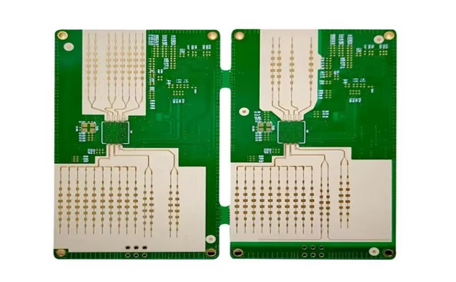
If you're looking to reduce costs in high-layer-count PCB design without sacrificing performance, you've come to the right place. High-layer-count PCBs, often used in complex electronics like servers, telecommunications equipment, and advanced medical devices, can be expensive due to material choices, layer complexity, and manufacturing processes. However, by focusing on smart design choices, material selection, and fabrication strategies, you can achieve significant cost savings. In this blog, we'll dive deep into the key cost drivers of high-layer-count PCBs, practical ways to lower fabrication expenses, and techniques for material cost optimization in PCB design. Let's explore how to balance performance and budget effectively.
Understanding High-Layer-Count PCB Cost Drivers
High-layer-count PCBs, typically defined as boards with 8 or more layers, are essential for applications requiring dense routing and high-speed signal integrity. However, their complexity directly impacts cost. To optimize expenses, it’s crucial to understand the primary factors driving up the price of these boards.
1. Number of Layers
The most obvious cost driver is the number of layers. Each additional layer increases material usage, manufacturing time, and the risk of defects during lamination. For example, a 12-layer PCB can cost 30-50% more than an 8-layer board due to the added copper and dielectric materials, as well as the precision needed in alignment during production.
2. Material Selection
High-layer-count PCBs often require advanced materials to maintain signal integrity at high frequencies (e.g., above 1 GHz). Materials like high-Tg FR-4 or low-loss laminates such as Rogers or Isola can double or triple material costs compared to standard FR-4. While these materials ensure performance, they significantly impact the budget.
3. Manufacturing Complexity
Complex designs with tight tolerances, such as controlled impedance traces (often requiring ±10% precision) or microvias, demand advanced fabrication techniques. These processes increase costs due to specialized equipment and longer production times. For instance, laser-drilled microvias, common in high-layer designs, can add 20-40% to fabrication costs compared to standard through-hole vias.
4. Board Size and Panel Utilization
Larger boards or inefficient panel layouts waste material, driving up costs. If a design doesn’t maximize the number of boards per panel, you’re essentially paying for unused space. Poor panelization can increase costs by 15-25%, especially for high-layer-count designs where material expenses are already high.
Strategies for PCB Fabrication Cost Reduction
Now that we know the key cost drivers, let’s focus on actionable strategies to reduce expenses during PCB fabrication without compromising quality or performance. These tips are tailored for high-layer-count designs and can be applied at various stages of the project.
1. Optimize Layer Count
While it might seem necessary to add layers for routing density, over-specifying the layer count can inflate costs unnecessarily. Review your design to see if routing can be optimized to reduce layers. For example, using wider traces or adjusting component placement might allow you to drop from 14 to 12 layers, saving 10-20% on fabrication costs. Use design software with layer optimization tools to simulate and test before finalizing the stack-up.
2. Simplify Routing and Minimize Vias
Complex routing with excessive vias, especially microvias or buried vias, increases drilling and plating costs. Aim to minimize via usage by optimizing trace paths. For high-speed designs, maintain signal integrity by keeping impedance consistent (e.g., 50 ohms for single-ended traces) rather than relying on additional vias for grounding. Simplifying via structures can cut costs by up to 15% in high-layer boards.
3. Standardize Specifications
Custom specifications, such as non-standard board thicknesses or unique surface finishes, often lead to higher costs due to setup changes in manufacturing. Stick to industry-standard specs wherever possible. For instance, using a standard 1.6mm board thickness instead of a custom 2.2mm can reduce costs by avoiding special handling, potentially saving 5-10% per board.
4. Improve Panel Utilization
Work with your manufacturer to optimize panel layouts. By fitting more boards onto a single panel, you reduce material waste and lower per-unit costs. For high-layer-count PCBs, even a 10% improvement in panel utilization can translate to significant savings, especially for small to medium production runs.
Material Cost Optimization in PCB Design
Material costs often account for 30-50% of the total expense in high-layer-count PCBs. Choosing the right materials and optimizing their use can lead to substantial savings while still meeting performance requirements.
1. Select Cost-Effective Laminates
While high-performance materials like low-loss laminates are necessary for applications with signal speeds above 5 Gbps, they’re overkill for less demanding designs. If your project operates at lower frequencies (e.g., below 1 GHz), standard FR-4 with a high-Tg rating (around 170°C) can suffice, cutting material costs by 20-30%. Always match the material to the application’s thermal and electrical needs.
2. Use Hybrid Stack-Ups
For designs requiring high-speed signals on specific layers, consider a hybrid stack-up. This approach combines expensive low-loss materials for critical signal layers with standard FR-4 for power and ground planes. A hybrid 10-layer board might use low-loss material only on layers 3 and 8 for high-speed traces, reducing material costs by 15-25% compared to a full low-loss stack-up.
3. Optimize Copper Weight
Thicker copper (e.g., 2 oz or 3 oz) is often used in high-layer-count PCBs for better current handling, but it increases costs due to higher material usage and etching challenges. Unless your design requires heavy copper for power distribution (e.g., currents above 5A), stick to 1 oz copper for signal layers. This can save 10-15% on copper costs while maintaining adequate performance.
4. Reduce Board Thickness Where Possible
Thicker boards use more dielectric material, driving up costs. If your design doesn’t require a specific thickness for mechanical strength or impedance control, opt for a thinner board. Reducing thickness from 2.0mm to 1.6mm in a 12-layer design can lower material costs by around 10%, provided it meets structural requirements.
Balancing Performance and Budget in High-Layer-Count Designs
Cost optimization doesn’t mean cutting corners that jeopardize performance. High-layer-count PCBs are often used in critical applications where signal integrity, thermal management, and reliability are non-negotiable. Here’s how to strike the right balance.
1. Prioritize Signal Integrity in Design
For high-speed applications, ensure that cost-saving measures like reducing layers or using cheaper materials don’t compromise signal quality. Maintain controlled impedance (e.g., 100 ohms for differential pairs) by adjusting trace width and spacing rather than opting for fewer layers. Use simulation tools to verify performance before fabrication, avoiding costly redesigns.
2. Focus on Thermal Management
High-layer-count PCBs often handle high power densities, leading to heat buildup. While thinner boards save costs, they may not dissipate heat effectively. If thermal performance is critical, incorporate thermal vias or copper pours strategically instead of increasing board thickness. This approach maintains reliability without significant cost increases.
3. Test Prototypes Before Full Production
Invest in small prototype runs to validate your cost-optimized design. Catching issues like signal crosstalk or thermal hotspots early prevents expensive revisions during mass production. For instance, testing a 10-layer board for signal integrity at 2.5 Gbps can confirm whether a cheaper material meets performance needs, saving thousands in potential rework costs.
Partnering with the Right Manufacturer for Cost Efficiency
The choice of manufacturing partner plays a critical role in cost optimization for high-layer-count PCBs. A reliable manufacturer can provide design feedback, suggest cost-effective alternatives, and ensure high-quality production. Look for partners who offer design for manufacturability (DFM) reviews to identify potential cost-saving opportunities, such as adjusting via sizes or improving panel layouts.
Additionally, consider production volume. For small runs, focus on manufacturers with low minimum order quantities to avoid overpaying for unused boards. For larger runs, negotiate bulk pricing to reduce per-unit costs. Transparent communication about your budget and performance needs can lead to tailored solutions that save money without sacrificing quality.
Conclusion: Achieving Cost-Effective High-Layer-Count PCB Designs
Designing high-layer-count PCBs on a budget is entirely possible with the right strategies. By understanding cost drivers like layer count, material selection, and manufacturing complexity, you can make informed decisions that lower expenses. Focus on optimizing layer usage, selecting cost-effective materials, and simplifying designs without compromising performance. Techniques like hybrid stack-ups, standardized specs, and efficient panelization offer practical ways to achieve savings. Finally, partnering with an experienced manufacturer ensures that your cost-optimized design is produced with precision and reliability.
Implementing these approaches allows you to balance performance and budget effectively, ensuring your high-layer-count PCBs meet both technical and financial goals. Whether you're working on telecommunications equipment or advanced computing systems, smart design and fabrication choices pave the way for success in complex electronics projects.
 ALLPCB


