ALLPCB


In the world of PCB manufacturing, precision and clarity in silkscreen printing are vital for creating high-quality boards. One of the most advanced methods to achieve this is Liquid Photo Imaging (LPI) on the top layer. If you're searching for ways to enhance silkscreen precision and achieve high-resolution results, LPI silkscreen offers a cutting-edge solution. This technique stands out for its ability to produce sharp, detailed markings that are essential for component identification and assembly accuracy.
In this comprehensive guide, we'll dive deep into the details of LPI silkscreen, exploring how liquid photo imaging works, its benefits in achieving silkscreen high resolution, and why it's considered one of the most advanced silkscreen techniques in PCB manufacturing. Whether you're an engineer, designer, or manufacturer, this blog will provide actionable insights to elevate your PCB production process.
What is Liquid Photo Imaging (LPI) in PCB Silkscreen?
Liquid Photo Imaging, often abbreviated as LPI, is a sophisticated silkscreen technique used to apply markings on the top layer of a printed circuit board (PCB). Unlike traditional manual silkscreen methods, LPI uses a photo-sensitive liquid ink that is applied to the PCB surface and then exposed to light through a photographic mask. This process allows for extremely fine details and high-resolution text or symbols, making it ideal for modern, complex PCB designs.
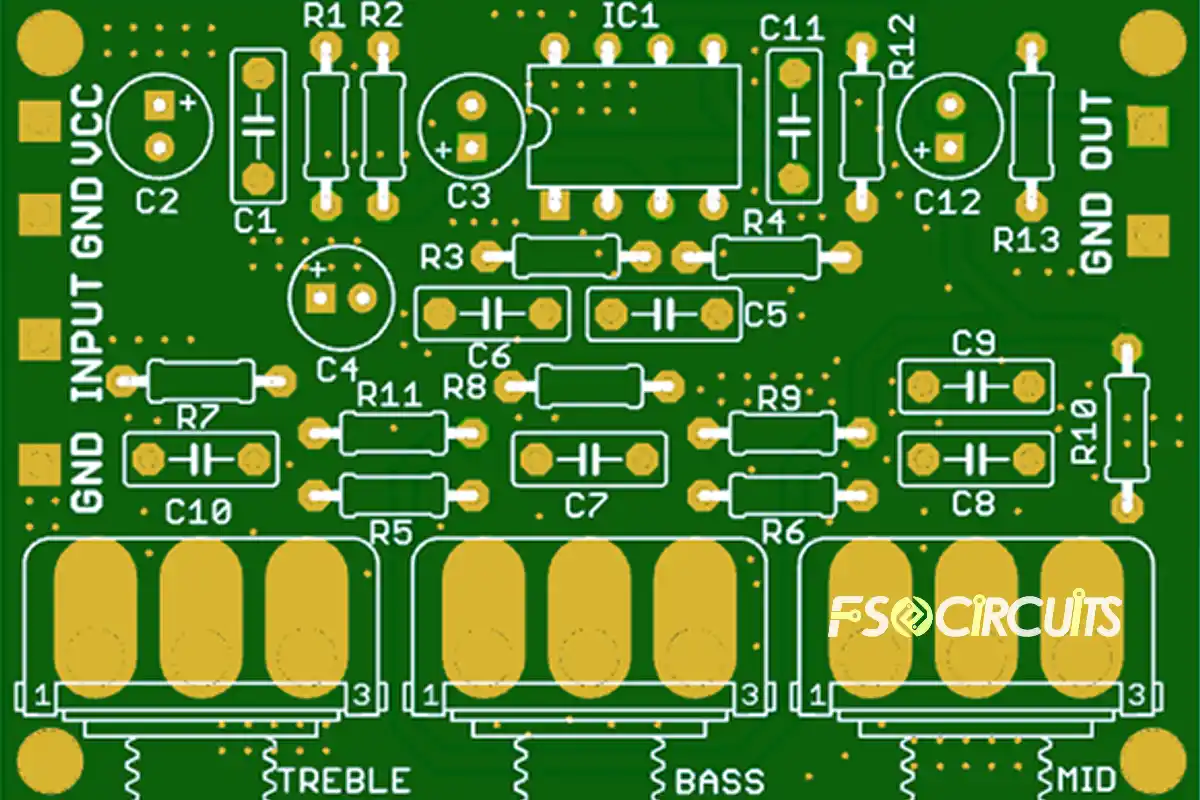
In PCB manufacturing, the silkscreen layer serves as a visual guide, displaying component designators, polarity markers, test points, and other critical information. With LPI silkscreen, these markings are not only clearer but also more durable, ensuring they remain legible even after exposure to harsh assembly processes or environmental conditions.
How Does Liquid Photo Imaging Work?
The LPI process in PCB manufacturing involves several precise steps to achieve silkscreen high resolution. Here's a breakdown of how it works:
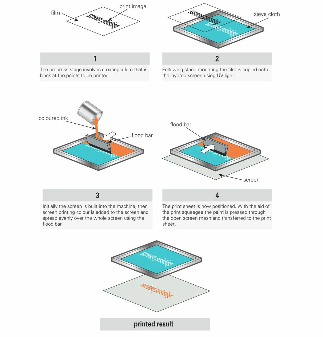
- Application of Photo-Sensitive Ink: A thin layer of liquid photo-sensitive ink is applied to the PCB's top layer. This ink is designed to harden when exposed to specific wavelengths of light.
- Photographic Mask Placement: A photographic mask, or film, containing the desired silkscreen design is placed over the ink-coated PCB. This mask blocks light in areas where markings are not needed.
- Light Exposure: The PCB is exposed to ultraviolet (UV) light. The areas of ink not covered by the mask harden due to the light exposure, while the covered areas remain soft.
- Development: After exposure, the PCB is washed with a developer solution that removes the unhardened ink, leaving behind the precise silkscreen pattern.
- Curing: The remaining ink is cured, often through heat or additional UV exposure, to ensure durability and resistance to wear during assembly and use.
This process allows for silkscreen precision down to very fine details, often achieving line widths as small as 0.075 mm (3 mils). Such accuracy is critical for densely populated PCBs where space for markings is limited.
Benefits of LPI Silkscreen in PCB Manufacturing
Liquid Photo Imaging offers several advantages over traditional silkscreen methods, making it a preferred choice for achieving silkscreen high resolution and precision in advanced PCB designs. Let's explore these benefits in detail:
1. Unmatched Silkscreen Precision
LPI silkscreen can produce extremely fine lines and small text, often below 0.1 mm in width. This level of precision is essential for modern PCBs with high component density, where even the smallest markings must be clear and legible. For example, on a board with surface-mount components spaced at 0.5 mm pitch, LPI ensures that reference designators remain distinct and useful for assembly.
2. High-Resolution Markings
The photographic process of LPI allows for silkscreen high resolution, meaning sharper and more detailed images, logos, and text. This is particularly useful for branding purposes or when intricate symbols are required to indicate polarity or specific test points.
3. Durability and Resistance
Once cured, LPI silkscreen markings are highly resistant to abrasion, chemicals, and heat. This durability ensures that critical information remains visible throughout the PCB's lifecycle, even during soldering processes that can reach temperatures of 260°C (500°F) or more.
4. Consistency Across Production Runs
Unlike manual silkscreen methods, which can vary due to human error, LPI uses a controlled photographic process. This results in consistent markings across large production runs, reducing the risk of errors in assembly due to unclear or misaligned labels.
5. Compatibility with Complex Designs
As PCB designs become more intricate, with smaller components and tighter spacing, LPI silkscreen adapts easily. It can place markings in tight spaces without sacrificing readability, supporting the trend toward miniaturization in electronics.
Comparing LPI to Other Silkscreen Techniques
To fully appreciate the value of LPI silkscreen, it's helpful to compare it with other common silkscreen advanced techniques used in PCB manufacturing. Here's how LPI stacks up against manual silkscreen and Direct Legend Printing (DLP):
- Manual Silkscreen: This traditional method involves pushing ink through a mesh screen onto the PCB. While cost-effective for simple designs, it lacks the precision and resolution of LPI, often resulting in thicker lines (above 0.15 mm) and less consistent results. It's also more prone to wear and smudging during handling.
- Direct Legend Printing (DLP): DLP uses an inkjet printer to apply markings directly onto the PCB. While faster than manual methods, it typically offers lower resolution than LPI, with line widths often limited to 0.1 mm or more. DLP markings can also be less durable under harsh conditions compared to LPI.
LPI stands out for its ability to combine silkscreen precision, high resolution, and durability, making it the go-to choice for high-end PCB applications such as aerospace, medical devices, and telecommunications equipment.
Applications of LPI Silkscreen in Modern PCB Manufacturing
The use of LPI silkscreen is particularly valuable in industries where precision and reliability are non-negotiable. Here are some key applications where this technique shines:
- High-Density Interconnect (HDI) Boards: HDI PCBs, used in smartphones and wearable devices, require precise markings due to their compact layouts. LPI ensures that even tiny reference designators (e.g., "R1" or "C2") are legible, aiding in assembly and debugging.
- Automotive Electronics: In automotive PCBs, where boards are exposed to vibration and temperature extremes, LPI silkscreen provides durable markings that withstand harsh environments.
- Medical Devices: For life-critical applications like pacemakers or diagnostic equipment, LPI offers the clarity needed for error-free assembly and maintenance.
- Aerospace Systems: Aerospace PCBs often feature complex designs with strict quality standards. LPI silkscreen ensures that every marking is precise, supporting traceability and compliance with regulations.
Challenges and Considerations with LPI Silkscreen
While LPI offers numerous advantages, there are some challenges to consider when adopting this technique in PCB manufacturing:
- Higher Cost: The LPI process involves specialized equipment and materials, making it more expensive than manual silkscreen methods. However, the cost is often justified by the improved quality and reduced error rates in assembly.
- Design Preparation: Creating the photographic mask for LPI requires precise design files. Any errors in the artwork can lead to incorrect markings, so thorough validation of the silkscreen layer in the design phase is essential.
- Processing Time: Compared to DLP, LPI can take longer due to the multiple steps involved (coating, exposure, development, and curing). This may impact production schedules for time-sensitive projects.
Despite these challenges, many manufacturers find that the benefits of silkscreen precision and high resolution outweigh the drawbacks, especially for high-stakes applications.
Tips for Optimizing LPI Silkscreen in Your PCB Design
To make the most of liquid photo imaging in your PCB projects, consider the following practical tips during the design and manufacturing stages:
- Use Appropriate Font Sizes: While LPI can achieve very small text, aim for a minimum height of 0.8 mm for readability under normal conditions. This ensures markings are visible without magnification during assembly.
- Minimize Clutter: Place only essential information on the silkscreen layer to avoid overcrowding. Focus on critical designators and polarity indicators, leaving out unnecessary details.
- Validate Artwork: Double-check the silkscreen layer in your design software to ensure alignment with component placements and board features. Misaligned markings can lead to assembly errors.
- Choose Contrasting Colors: Typically, white ink on a green or blue solder mask offers the best contrast for LPI silkscreen. Ensure the color choice maximizes visibility under various lighting conditions.
- Collaborate with Your Manufacturer: Work closely with your PCB fabrication partner to confirm that their LPI process aligns with your design requirements, especially for line width and spacing tolerances.
By following these guidelines, you can leverage silkscreen advanced techniques like LPI to enhance the quality and functionality of your PCBs.
Future Trends in Silkscreen Techniques and LPI
As PCB manufacturing continues to evolve, so do silkscreen advanced techniques. The future of LPI silkscreen looks promising, with ongoing innovations aimed at further improving precision and efficiency. Some emerging trends include:
- Automation in LPI Processes: Advances in automation are reducing the time and cost associated with LPI, making it more accessible for smaller production runs.
- Integration with Digital Tools: New software tools are simplifying the design-to-production workflow for LPI, allowing designers to simulate silkscreen results before fabrication.
- Eco-Friendly Materials: Research is underway to develop more sustainable photo-sensitive inks for LPI, reducing the environmental impact of PCB manufacturing.
These developments suggest that LPI silkscreen will remain a cornerstone of high-quality PCB production, adapting to meet the demands of increasingly complex electronics.
Conclusion: Why Choose LPI Silkscreen for Your Next PCB Project?
Liquid Photo Imaging (LPI) represents a significant leap forward in silkscreen advanced techniques, offering unmatched silkscreen precision and high resolution for PCB manufacturing. Its ability to produce fine, durable markings makes it an ideal choice for modern, high-density designs across industries like automotive, medical, and aerospace. While it comes with a higher cost and additional design considerations, the benefits of clarity, consistency, and reliability often outweigh these challenges.
At ALLPCB, we are committed to providing cutting-edge solutions for your PCB needs, including advanced LPI silkscreen techniques. By incorporating LPI into your designs, you can ensure that your boards meet the highest standards of quality and functionality. Whether you're working on a prototype or a large-scale production run, this method can elevate your project to the next level.