 ALLPCB


In today’s world, where technology drives almost every aspect of life, the environmental impact of electronics manufacturing cannot be ignored. Printed Circuit Boards (PCBs), the backbone of electronic devices, have a significant effect on the planet due to the materials and processes involved in their production. So, how does green PCB production help reduce this impact? By adopting eco-conscious practices, the industry can minimize pollution, lower chemical usage, and promote water conservation, paving the way for a sustainable future. In this blog, we’ll dive deep into the environmental challenges of PCB manufacturing and explore how green initiatives are making a difference with practical solutions and real data.
Understanding the Environmental Impact of Traditional PCB Production
Traditional PCB manufacturing has long been associated with environmental challenges. The process involves multiple stages, including material extraction, chemical etching, and waste disposal, each contributing to pollution and resource depletion. Let’s break down the key issues:
- Heavy Chemical Usage: PCB production often relies on harsh chemicals like acids and solvents for etching copper layers and cleaning boards. These substances can contaminate water sources if not handled properly. Studies suggest that untreated wastewater from PCB plants can contain high levels of copper and other heavy metals, posing risks to aquatic life.
- Water Consumption: Manufacturing a single PCB can require significant amounts of water for rinsing and cooling processes. Without proper recycling systems, this leads to excessive water waste, a critical concern in regions facing water scarcity.
- Energy-Intensive Processes: The production of PCBs demands substantial energy for machinery and heating, often sourced from non-renewable fuels. This contributes to greenhouse gas emissions, with some estimates indicating that electronics manufacturing accounts for roughly 2-3% of global carbon emissions.
- Non-Recyclable Waste: Many traditional PCBs use materials that are difficult to recycle, leading to e-waste accumulation in landfills. This waste can release toxic substances over time, further harming the environment.
What Is Green PCB Production?
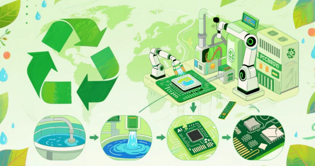
Green PCB production focuses on eco-conscious methods to minimize environmental harm. It involves using sustainable materials, reducing chemical usage, conserving water, and adopting energy-efficient practices. The goal is to create PCBs that meet performance standards while having a lower green impact on the planet. This approach aligns with global regulations like RoHS (Restriction of Hazardous Substances), which limits the use of toxic materials in electronics.
By prioritizing sustainability, manufacturers can reduce pollution and create a positive ripple effect across the supply chain. For engineers and businesses, choosing eco-conscious PCB solutions means contributing to a cleaner environment without sacrificing quality or efficiency.
How Eco-Conscious PCB Production Reduces Pollution
One of the primary benefits of green PCB production is its ability to reduce pollution at various stages. Here’s how eco-conscious practices make a difference:
- Minimizing Toxic Emissions: By replacing harmful chemicals with biodegradable or less toxic alternatives, manufacturers can lower air and water pollution. For instance, some companies now use water-based inks for PCB printing instead of solvent-based options, cutting down volatile organic compound (VOC) emissions by up to 50% in certain cases.
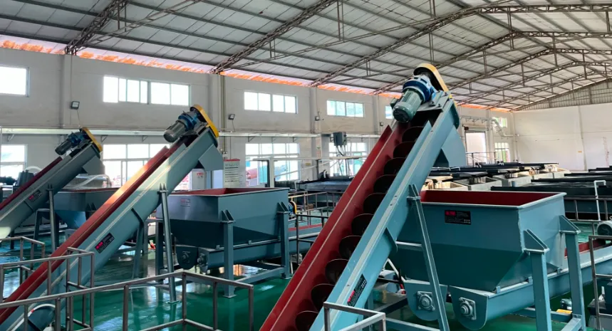
- Recycling Waste Materials: Eco-conscious production emphasizes recycling scrap materials like copper and laminate offcuts. This prevents waste from ending up in landfills and reduces the need for raw material extraction, which often involves destructive mining practices.
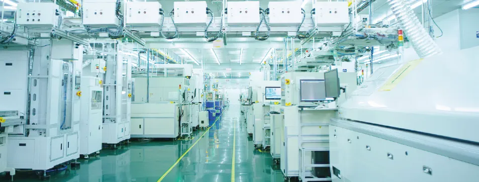
- Energy Efficiency: Modern green manufacturing facilities use energy-efficient machinery and renewable energy sources like solar or wind power. This can reduce carbon footprints significantly, with some plants reporting a 30-40% drop in energy consumption after adopting sustainable technologies.
Cutting Down Chemical Usage in Green PCB Manufacturing
Chemical usage is a major concern in PCB production, but green initiatives are addressing this issue head-on. Here are some strategies being implemented to reduce reliance on harmful substances:
- Lead-Free Soldering: Traditional soldering often uses lead, a toxic metal that can harm both the environment and human health. Green PCB production adopts lead-free solder alloys, such as tin-silver-copper mixtures, which are safer and comply with global standards. While lead-free soldering may require slightly higher melting temperatures (around 217-220°C compared to 183°C for lead-based solder), the environmental benefits outweigh the challenges.
- Alternative Etching Solutions: Instead of using strong acids for etching copper layers, some manufacturers are exploring less toxic options or dry etching techniques that produce minimal chemical waste. This reduces the risk of water contamination and lowers disposal costs.
- Closed-Loop Systems: Advanced facilities use closed-loop chemical systems to recycle and reuse chemicals within the production process. This can cut chemical waste by up to 70%, based on data from sustainable manufacturing reports.
By focusing on these methods, the industry is taking significant steps to limit the environmental damage caused by chemical usage, ensuring safer production for workers and the planet alike.
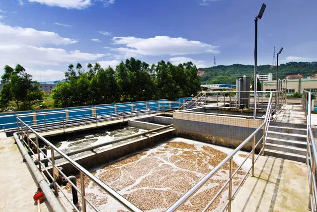
Water Conservation in Eco-Conscious PCB Production
Water conservation is another critical aspect of green PCB manufacturing. Traditional processes consume large volumes of water, but sustainable practices are changing the game. Here’s how:
- Water Recycling Systems: Many eco-conscious facilities install systems to treat and reuse wastewater from rinsing and cleaning stages. This can reduce water usage by as much as 60%, according to industry studies, making a huge difference in water-scarce regions.
- Optimized Processes: By redesigning production workflows, manufacturers can minimize water-intensive steps. For example, using high-pressure rinsing nozzles instead of standard ones can cut water consumption by 20-30% without affecting quality.
- Rainwater Harvesting: Some plants incorporate rainwater harvesting to supplement their water needs for non-critical processes. This reduces reliance on municipal water supplies and supports local ecosystems.
The Role of Sustainable Materials in Green PCB Production
Materials play a vital role in determining the green impact of PCB production. Traditional boards often use non-biodegradable substrates and hazardous coatings, but sustainable alternatives are gaining traction. Here are some innovations in this area:
- Biodegradable Substrates: Researchers and manufacturers are developing PCBs made from biodegradable materials like cellulose-based composites. These materials break down naturally over time, reducing long-term e-waste. While still in early adoption, they show promise for low-power applications.
- Recyclable Laminates: Using laminates that can be easily separated and recycled helps recover valuable materials like copper. This cuts down on waste and reduces the need for virgin resources.
- Halogen-Free Materials: Halogens like bromine and chlorine, often used in flame-retardant coatings, can release toxic fumes when burned. Halogen-free alternatives provide the same safety benefits without the environmental risks, aligning with eco-conscious goals.
Switching to sustainable materials not only lowers the environmental footprint but also meets the growing demand for greener electronics among consumers and businesses.
Benefits of Green PCB Production for Businesses and Engineers
Adopting eco-conscious PCB production offers numerous advantages beyond environmental benefits. For businesses and engineers, going green can be a strategic move:
- Cost Savings: Energy-efficient processes and water recycling systems reduce operational costs over time. For instance, a facility that cuts energy use by 30% can save thousands of dollars annually on utility bills.
- Regulatory Compliance: Meeting standards like RoHS and REACH (Registration, Evaluation, Authorization, and Restriction of Chemicals) ensures that products can be sold in global markets without legal hurdles.
- Enhanced Reputation: Companies that prioritize sustainability often gain a competitive edge by appealing to environmentally conscious customers and partners.
- Innovation Opportunities: Engineers working with green materials and processes can develop cutting-edge solutions, such as boards with improved thermal performance (e.g., thermal conductivity of 0.5-1 W/mK for certain eco-friendly substrates) or reduced signal loss at high frequencies.
Challenges in Implementing Green PCB Production
While the benefits are clear, transitioning to eco-conscious PCB production isn’t without challenges. Understanding these hurdles can help stakeholders prepare for a smoother shift:
- Higher Initial Costs: Investing in sustainable equipment and materials often requires upfront capital. For example, installing a water recycling system might cost tens of thousands of dollars, though long-term savings offset this.
- Technical Limitations: Some green materials may not yet match the performance of traditional options in high-stress or high-frequency applications. Ongoing research aims to close this gap.
- Supply Chain Adjustments: Sourcing sustainable materials and ensuring suppliers follow eco-friendly practices can be complex, especially for smaller manufacturers.
Despite these obstacles, the industry is moving forward with innovative solutions and government support, making green production more accessible every day.
Future Trends in Eco-Conscious PCB Manufacturing
The future of green PCB production looks promising, with several trends shaping the industry’s path toward sustainability:
- Digital Twin Technology: Using digital simulations to optimize manufacturing processes can reduce material waste and energy use by up to 25%, based on early case studies.
- Circular Economy Models: Emphasizing reuse and recycling, circular economy principles aim to keep materials in use for as long as possible, minimizing waste.
- Advanced Biodegradable Boards: As research progresses, we can expect biodegradable PCBs to become viable for a wider range of applications, potentially revolutionizing e-waste management.
Conclusion: Building a Sustainable Future with Green PCB Production
Green PCB production is more than a trend—it’s a necessary step toward reducing the environmental impact of electronics manufacturing. By focusing on eco-conscious practices, the industry can tackle pollution, cut down on chemical usage, and prioritize water conservation while still delivering high-quality products. For engineers and businesses, adopting sustainable methods not only helps the planet but also brings cost savings, compliance benefits, and innovation opportunities.
As technology evolves, the push for greener solutions will only grow stronger. By staying ahead of the curve and embracing these changes, we can collectively build a future where technology and sustainability go hand in hand. Whether you’re designing a new circuit or sourcing components, consider the green impact of your choices and opt for eco-conscious PCB solutions whenever possible.


