 ALLPCB


In the world of printed circuit board (PCB) design, moving beyond traditional rectangular shapes opens up exciting possibilities for innovation. But how do you handle the manufacturing challenges of non-rectangular PCB or non-standard PCB shapes? Advanced V-scoring techniques, including jump scoring and breakaway tabs, offer practical solutions for separating these unique designs from production panels with precision and efficiency. In this blog, we’ll explore how these advanced PCB scoring methods work, why they’re essential for non-standard shapes, and how they can streamline your manufacturing process.
Whether you’re an engineer working on a cutting-edge wearable device or designing a custom PCB for a niche application, understanding these techniques can save time, reduce costs, and ensure high-quality results. Let’s dive into the details of V-scoring for non-standard PCB shapes and uncover the tools and strategies that make it possible.
What Is V-Scoring and Why Does It Matter for Non-Standard PCB Shapes?
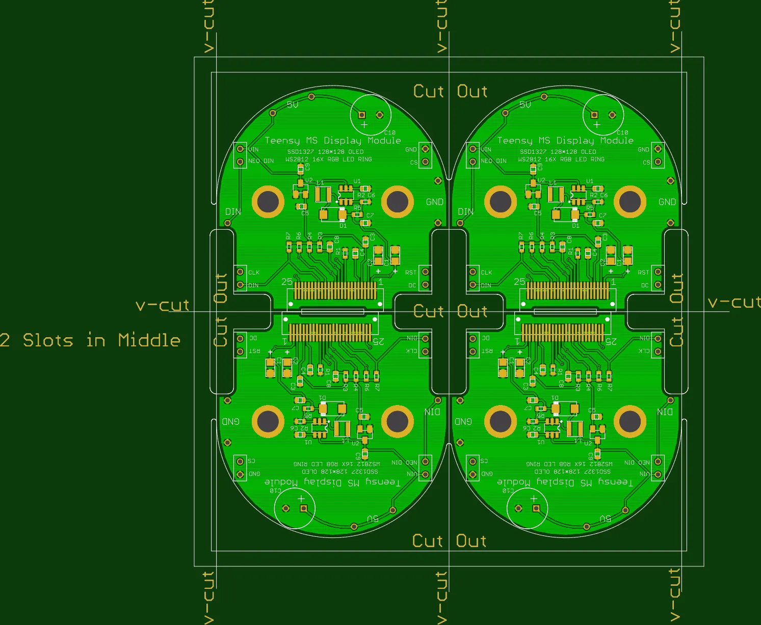
V-scoring, also known as V-grooving or V-cutting, is a widely used method in PCB manufacturing to facilitate the separation of individual boards from a larger production panel. This technique involves cutting V-shaped grooves into both the top and bottom sides of the panel, leaving a thin layer of material that can be easily snapped apart after assembly. For rectangular PCBs, V-scoring is straightforward and highly effective. However, when it comes to non-rectangular PCB or non-standard PCB designs, traditional V-scoring often falls short due to irregular edges and complex geometries.
Non-standard PCB shapes are increasingly common in industries like wearables, IoT devices, and automotive electronics, where space constraints and aesthetic requirements demand unique form factors. Think of a circular PCB for a smartwatch or a polygonal board for a sensor module. These shapes pose unique challenges during panelization and separation, as straight V-cuts may not align with curved or angled edges. This is where advanced PCB scoring techniques come into play, ensuring clean breaks without damaging delicate components or traces near the edges.
Challenges of Scoring Non-Rectangular PCB Designs
Before we explore advanced techniques, it’s important to understand the specific challenges that non-standard PCB shapes present during scoring and separation. These challenges include:
- Irregular Edges: Unlike rectangular boards, non-rectangular PCBs often have curved or angled edges that don’t align with straight V-scoring lines. This can lead to uneven stress during separation, risking damage to the board.
- Component Proximity: In compact non-standard designs, components and traces are often placed close to the edges. Traditional scoring can cause microcracks or mechanical stress, affecting performance.
- Panel Stability: Non-standard shapes can make it difficult to maintain panel integrity during manufacturing processes like soldering or testing, as irregular layouts may weaken the panel structure.
- Separation Precision: Achieving clean breaks without residual material or rough edges is harder with non-standard geometries, potentially requiring additional finishing steps.
These challenges highlight the need for specialized scoring methods tailored to non-standard PCB shapes. Let’s look at how advanced V-scoring techniques address these issues.
Advanced V-Scoring Techniques for Non-Standard PCB Shapes
Advanced PCB scoring goes beyond traditional V-cuts to accommodate the unique demands of non-rectangular designs. Below, we’ll cover key methods like jump scoring and breakaway tabs, along with practical tips for implementation.
1. Jump Scoring: Precision for Complex Geometries
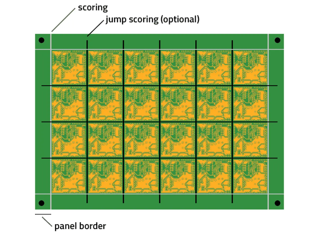
Jump scoring, also known as skip scoring, is a variation of V-scoring designed to handle non-standard PCB shapes more effectively. Unlike continuous V-cuts, jump scoring creates intermittent grooves along the separation line, leaving small uncut sections in between. These uncut areas provide additional stability to the panel during manufacturing, preventing premature detachment or damage to irregular shapes.
For non-rectangular PCBs, jump scoring is particularly useful because it allows manufacturers to strategically place grooves only where separation is feasible, avoiding areas with critical components or complex curves. For example, on a circular PCB, jump scoring might be applied in short segments along the perimeter, ensuring the board remains secure in the panel until the final separation stage.
Key Benefits of Jump Scoring for Non-Standard Shapes:
- Enhanced panel stability during assembly and testing.
- Reduced risk of damage to delicate edges or nearby components.
- Customizable scoring patterns to match unique board outlines.
2. Breakaway Tabs: Flexibility for Irregular Designs
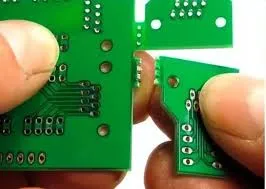
Breakaway tabs, sometimes called mousebites, are another essential technique for non-standard PCB shapes. Instead of relying solely on V-scoring, breakaway tabs use small perforated bridges to connect individual boards to the panel. These tabs are designed to be strong enough to hold the PCB in place during manufacturing but weak enough to be snapped off by hand or with minimal force after assembly.
For non-rectangular PCBs, breakaway tabs offer unmatched flexibility. They can be placed at strategic points along irregular edges, ensuring that even the most complex shapes remain secure in the panel. Additionally, the perforations in breakaway tabs minimize mechanical stress during separation, reducing the likelihood of cracks or damage. This method is often combined with V-scoring for optimal results, where V-cuts handle straight sections and tabs support curved or angled areas.
Design Tips for Breakaway Tabs:
- Place tabs away from sensitive components to avoid stress-related damage.
- Use 3-5 small perforations per tab for a balance of strength and easy removal.
- Space tabs evenly along the board’s perimeter to distribute stress during separation.
3. Hybrid Scoring Approaches for Maximum Efficiency
In many cases, a combination of V-scoring, jump scoring, and breakaway tabs delivers the best results for non-rectangular PCB designs. This hybrid approach allows manufacturers to tailor the separation method to the specific geometry of the board. For instance, straight sections of a polygonal PCB might use traditional V-scoring, while curved or irregular areas could rely on jump scoring or breakaway tabs.
Hybrid scoring also optimizes manufacturing efficiency. By minimizing the number of continuous cuts, it reduces tool wear and speeds up the scoring process. Additionally, it lowers the risk of panel instability, which is a common concern with non-standard shapes. When designing your PCB, work closely with your manufacturer to determine the best mix of scoring techniques based on your board’s layout and material properties (e.g., FR-4 thickness or copper weight).
Best Practices for Designing Non-Standard PCBs with Advanced Scoring
To make the most of advanced PCB scoring techniques, careful design and planning are essential. Here are some actionable best practices to follow when working with non-rectangular or non-standard PCB shapes:
- Optimize Panel Layout: Arrange non-standard PCBs on the panel to minimize wasted space while ensuring enough room for scoring lines and tabs. Consider nesting irregular shapes to maximize material usage.
- Define Scoring Specifications: Clearly specify the depth and angle of V-scoring grooves in your design files. For FR-4 boards with a thickness of 1.6mm, a typical V-cut depth might be 0.4mm on each side, leaving a 0.8mm residual layer for separation.
- Avoid Critical Areas: Keep scoring lines and breakaway tabs at least 2-3mm away from components, vias, and traces to prevent damage from mechanical stress. This is especially important for high-density designs.
- Test Prototypes: Before full-scale production, create a prototype panel to test your scoring setup. Check for clean breaks, edge quality, and any signs of stress or damage near scoring lines.
- Communicate with Manufacturers: Provide detailed documentation and collaborate with your manufacturing partner to ensure they understand your scoring requirements for non-standard shapes.
Benefits of Advanced Scoring for Non-Standard PCB Manufacturing
Implementing advanced V-scoring techniques like jump scoring and breakaway tabs offers several advantages for non-rectangular PCB production:
- Improved Yield Rates: Precise scoring reduces the risk of damaged boards during separation, leading to higher manufacturing yields. This is critical for cost-sensitive projects.
- Faster Production Cycles: Efficient panelization and separation methods streamline the manufacturing process, cutting down on production time.
- Enhanced Design Freedom: Advanced scoring empowers engineers to push the boundaries of PCB design, creating innovative non-standard shapes without sacrificing manufacturability.
- Cost Savings: By minimizing material waste and reducing the need for secondary finishing processes, these techniques help keep production costs in check.
Real-World Applications of Non-Standard PCB Scoring
Non-rectangular PCBs with advanced scoring techniques are making waves across various industries. Here are a few examples of how these methods are applied:
- Wearable Technology: Circular or oval PCBs for smartwatches and fitness trackers use jump scoring and breakaway tabs to fit unique enclosures while maintaining panel stability during assembly.
- Automotive Electronics: Custom-shaped PCBs for sensors and control modules often rely on hybrid scoring to handle complex geometries and tight tolerances.
- IoT Devices: Compact, non-standard boards for IoT gadgets benefit from precise scoring to ensure clean separation without compromising small form factors.
These applications demonstrate the versatility and importance of advanced PCB scoring in modern electronics design. By mastering these techniques, engineers can bring even the most ambitious designs to life.
Conclusion: Pushing the Boundaries with Advanced PCB Scoring
As PCB designs continue to evolve beyond traditional rectangles, advanced V-scoring techniques like jump scoring and breakaway tabs are becoming indispensable tools for engineers and manufacturers. These methods address the unique challenges of non-rectangular PCB and non-standard PCB shapes, ensuring precise separation, high-quality edges, and efficient production. By incorporating these strategies into your design workflow, you can unlock new possibilities for innovation while maintaining reliability and cost-effectiveness.
Whether you’re working on a groundbreaking wearable, a compact IoT device, or a custom automotive module, understanding and applying advanced PCB scoring is the key to success. Take the time to plan your panelization, collaborate with your manufacturing partner, and test your designs to achieve the best results. With the right approach, there’s no limit to the shapes and solutions you can create.


