 ALLPCB


Introduction
Wave soldering continues to play a critical role in through-hole component assembly, offering high throughput for medium to high-volume production. When combined with PCB panelization, this process amplifies efficiency by allowing multiple boards to be processed simultaneously through the solder wave. However, improper design in panelization can lead to defects such as bridging, insufficient fill, or warpage, compromising yield and reliability. Electrical engineers must consider factors like component orientation, thermal management, and structural integrity to achieve optimal results. This article delves into key design considerations for PCB panelization wave soldering, drawing on established engineering principles to guide better outcomes. By addressing these elements early in the design phase, teams can minimize rework and ensure consistent solder joint quality.
Understanding Wave Soldering and PCB Panelization
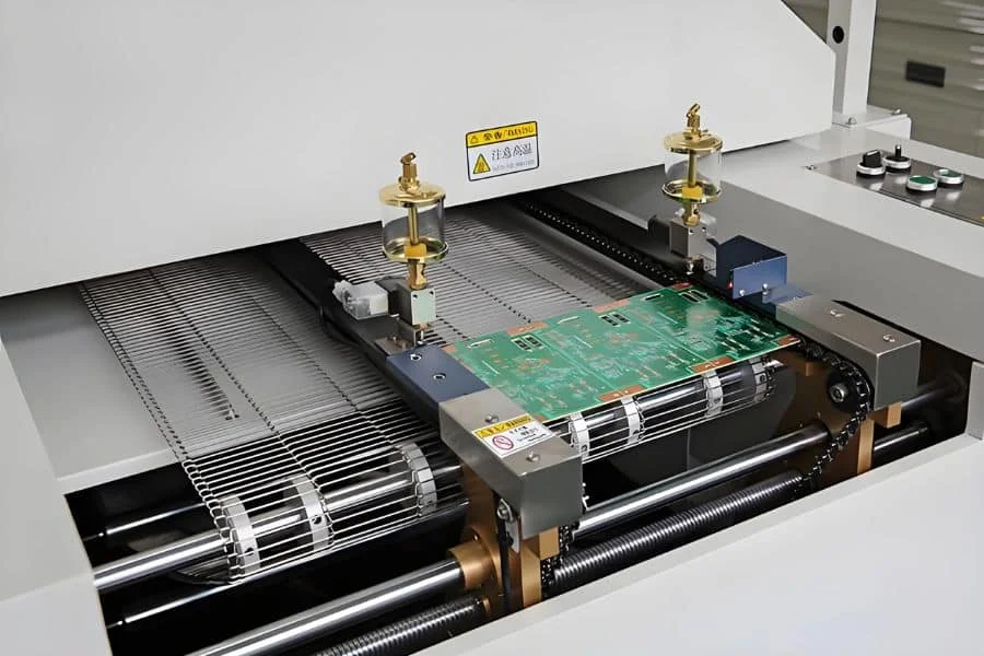
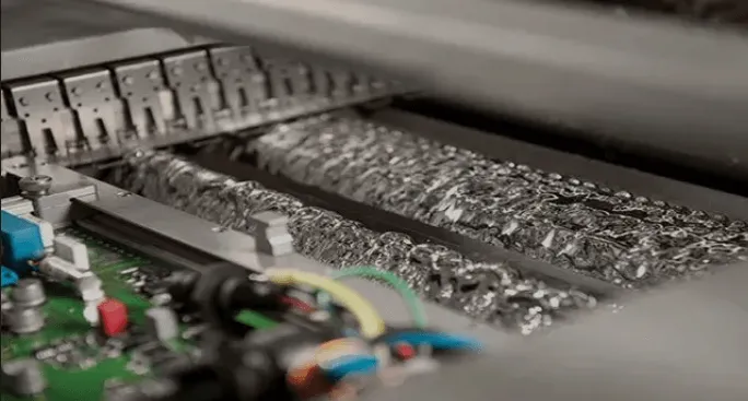
Wave soldering involves conveying a PCB over a molten solder bath, where a pumped wave contacts the underside to form joints on through-hole leads. The process typically includes flux application, preheating to activate flux and prevent thermal shock, and the solder contact stage, followed by cooling. PCB panelization groups individual boards into a larger array using methods like v-scoring, tab routing, or perforations, enabling automated handling and depaneling post-assembly. This approach reduces setup times and material waste but introduces challenges like uneven heating across the panel due to varying board densities. Industry relevance stems from cost savings in high-volume runs, yet success hinges on design alignment with process dynamics. For electrical engineers, grasping these fundamentals ensures panels withstand conveyor transport and wave exposure without distortion.
Panelization methods influence wave soldering performance significantly. V-scoring suits rectangular arrays with straight breaks, while tab routing offers flexibility for irregular shapes but requires precise mouse bites for clean separation. Fiducial marks on panels aid machine vision for alignment during fluxing and soldering. Poor panel design can exacerbate issues like solder flooding on unsupported edges or shadow effects from tall components. Standards such as IPC-2221 provide generic guidelines for printed board design, emphasizing layout that supports manufacturing flows. Electrical engineers benefit from integrating these insights to balance electrical performance with assembly feasibility.
Key Technical Principles in Wave Soldering with Panels
Solder flow in wave soldering follows principles of capillary action and surface tension, where molten solder wets pads and climbs vias or leads under controlled conditions. Preheat ensures uniform temperature rise, mitigating risks like delamination in multilayer panels. Panel size affects dwell time over the wave; larger panels may require adjusted conveyor speeds to maintain consistent contact. Thermal gradients across the panel arise from copper density variations, influencing barrel fill in plated through-holes. Ground planes act as heat sinks, potentially causing cold joints if not managed. Understanding these mechanisms allows engineers to predict defect modes and refine designs proactively.
Component leads interact with the wave dynamically, with solder meniscus formation dictating fillet quality. In panelized arrays, edge boards experience different airflow and radiation compared to inner ones, amplifying warpage risks from asymmetric cooling. Via geometry impacts solder wicking, where open vias near the solder side draw excess material, starving joints. Flux residues must evaporate fully during preheat to avoid corrosion, a factor compounded by panel thickness variations. These principles underscore the need for holistic design review before fabrication. By modeling heat transfer and flow, engineers can simulate outcomes without physical prototypes.
Design Considerations for Component Orientation in Wave Soldering
Component orientation profoundly affects solder distribution in PCB panelization wave soldering. Leads should face the direction of board travel to promote even wetting, avoiding turbulence that causes bridging. Tall components positioned perpendicular to the conveyor can shadow downstream parts, leading to dry joints. Orient polarized devices consistently across the panel to streamline inspection and reduce handling errors post-depaneling. Electrical engineers should prioritize signal integrity alongside this, ensuring critical paths avoid wave-induced stress concentrations. Simulations of airflow over the panel help validate orientations before commit.
In mixed technology panels with both through-hole and surface mount, orientation minimizes top-side flooding from solder balls. Low-profile parts near edges benefit from inward facing to counter capillary pull. Panel rail supports prevent sagging, maintaining parallelism to the wave. Deviations as small as a few degrees alter dwell time per lead row. Documenting orientation rules in design files ensures consistency across revisions. This structured approach aligns mechanical stability with joint reliability.
Thermal Reliefs and Panel Design Optimization
Thermal relief panel design addresses heat dissipation challenges during wave soldering. Solid connections to ground or power planes rob heat from pads, resulting in incomplete wetting or voids. Spoke-style reliefs, typically 90-degree segments, balance thermal conductivity while allowing solder flow. Wider spokes suit higher current paths, but over-design risks overheating sensitive components. In panels, uniform relief application prevents hot spots that warp substrates unevenly. Engineers must calculate relief geometry based on copper weight and layer stackup for predictable performance.
IPC J-STD-001 outlines requirements for soldered assemblies, including criteria for thermal relief efficacy in through-hole joints. Panels demand consistent pad sizes across arrays to avoid preheat imbalances. Test coupons on panels verify relief performance under production conditions. Overly aggressive reliefs compromise mechanical strength, so balance is key. Integrating these into design checklists elevates yield. Factory insights confirm that optimized reliefs reduce touch-up by significant margins without quantified claims.

Ground Plane Considerations in Wave Soldering
Ground plane considerations wave soldering require careful management to prevent thermal robbing. Solid copper pours under pins extract heat rapidly, slowing solder rise and causing barrel voids. Partial etching or relief breaks in planes maintain reference integrity while aiding fill. In panelized layouts, plane continuity across score lines must support depaneling stresses without cracking. Multilayer boards amplify effects, as inner planes conduct heat laterally. Engineers model plane coverage to predict joint temperatures accurately.
Stitching vias around planes distribute heat but risk wicking if untented. Solder mask dams over planes control excess flow onto topside. Panel edges benefit from thinned planes to match inner board heating. Compliance with design standards ensures electromagnetic compatibility alongside solderability. Iterative dfm reviews catch plane-related issues early. This proactive stance minimizes field failures from marginal joints.
Via Placement and Other Panel Design Factors
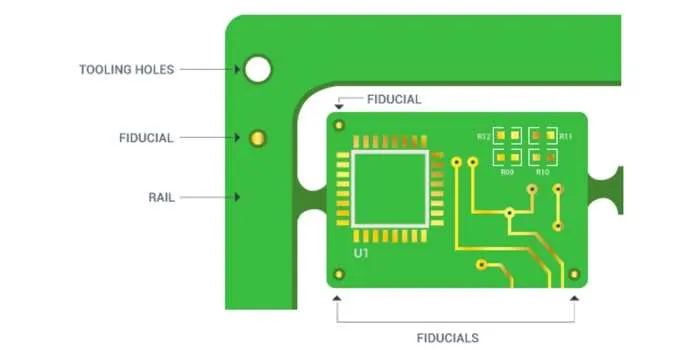
Via placement panel design influences solder entrapment and joint voids in wave soldering. Position vias away from pad edges to curb wicking, tenting solder-side masks where feasible. Blind or buried vias reduce exposure, but through-vias need annular rings sized per process capabilities. In panels, cluster vias sparingly to avoid localized cooling. Fiducials and tooling holes placement ensures conveyor stability, typically 0.1 inches from edges. V-groove depth controls break strength without splintering during wave flexure.
Spacing between boards in panels prevents cross-contamination from flux spray or solder splash. Minimum 0.2-inch gaps accommodate component heights and allow airflow. Asymmetric loading from heavy grounds on one side induces warpage, countered by balanced copper distribution. Mouse bites in tabs facilitate depaneling without stressing wave joints. Electrical engineers integrate these with routing for signal integrity. Comprehensive guidelines yield robust panels.
Best Practices for Implementation
Adopt a dfm workflow starting with panel array optimization software to visualize wave paths. Standardize component libraries with pre-verified orientations and reliefs. Prototype small panels to baseline process windows before scaling. Monitor preheat profiles across panel zones, adjusting ramps for uniformity. Post-solder x-ray or cross-section analysis validates designs per IPC-A-610 acceptability classes. Collaborate with fabricators on stackup tolerances to control warpage under 0.75% typically.
Incorporate breakaway tabs with rounded corners to distribute shear forces evenly. Use non-functional pads for strain relief near scores. For high-density panels, limit to 8-12 boards per array based on conveyor width. Document all deviations from standards for traceability. These practices, rooted in factory experience, drive consistent results. Engineers gain confidence through data-driven iterations.
Conclusion
Effective PCB panelization wave soldering demands integrated design thinking across component orientation wave soldering, thermal relief panel design, ground plane considerations wave soldering, and via placement panel design. By aligning layouts with process physics and standards like IPC-2221 and J-STD-001, electrical engineers mitigate defects and boost throughput. Key takeaways include balanced copper distribution, edge clearances, and simulation validation. Implementing these considerations early pays dividends in yield and reliability. Future designs will evolve with lead-free alloys, but core principles endure. Prioritize structured reviews for sustained success.
FAQs
Q1: What are the best practices for component orientation wave soldering in panelized PCBs?
A1: Orient through-hole leads parallel to the conveyor direction to ensure even solder contact and minimize shadowing. Keep tall components upstream to avoid blocking flux or wave on downstream parts. Maintain consistent polarity across the panel for efficient handling. This approach, aligned with soldering standards, reduces bridging and improves fillet formation in high-volume runs. Panels with optimized orientation see fewer rework needs during production.
Q2: How do thermal reliefs impact panel design for wave soldering?
A2: Thermal reliefs in pad designs prevent excessive heat sinking from ground planes, promoting complete barrel fill. Use 90-degree spokes sized to copper thickness for balanced performance. Uniform application across panels avoids thermal gradients and warpage. Engineers should verify via thermal profiling to match process windows. Proper reliefs enhance joint reliability without sacrificing electrical integrity.
Q3: Why are ground plane considerations wave soldering critical in panels?
A3: Ground planes rob heat from joints, risking cold solder in wave processes. Incorporate reliefs or breaks under pins to allow proper wetting. Balance plane density symmetrically in panels to prevent distortion. This maintains emc while supporting assembly yields. Design reviews focusing on these ensure robust performance.
Q4: What via placement strategies optimize panel design for wave soldering?
A4: Place vias inward from pad edges and tent solder-side to limit wicking. Avoid clusters that cool localized areas unevenly. Account for annular ring sizes in panel arrays for consistent plating. These steps minimize voids and excess solder, aligning with manufacturing flows. Balanced placement supports high-reliability assemblies.
References
IPC-2221A — Generic Standard on Printed Board Design. IPC, 1998
IPC J-STD-001G — Requirements for Soldered Electrical and Electronic Assemblies. IPC, 2017
IPC-A-610H — Acceptability of Electronic Assemblies. IPC, 2019


