 ALLPCB


Introduction
Ball grid array (BGA) components dominate modern high-density electronics due to their compact footprint and high I/O count. As PCB designs push toward finer pitches below 0.65 mm, traditional fanout strategies struggle to provide sufficient routing channels. Via-in-pad BGA design emerges as a critical technique, placing vias directly within BGA pads to maximize routing density and enable efficient BGA escape routing. This approach supports via-in-pad BGA configurations essential for electric engineers tackling complex multilayer boards. Key considerations span via sizing, filling processes, fanout patterns, and soldering reliability to ensure signal integrity and manufacturability. Mastering these elements aligns with industry demands for reliable high-performance PCBs.
Understanding Via-in-Pad Design for BGA Components
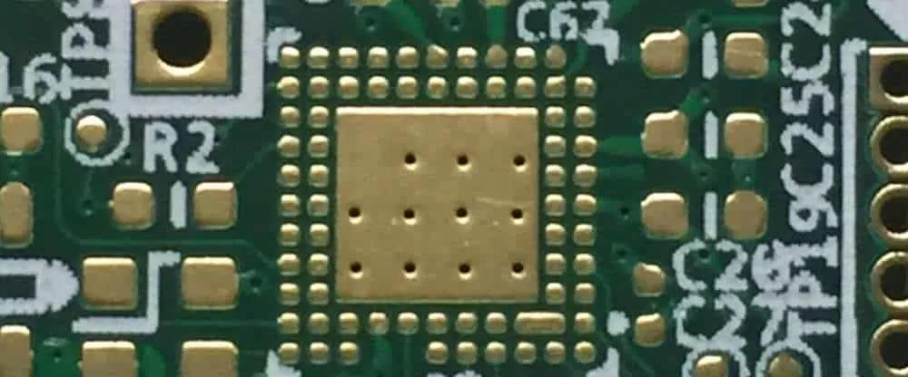
Via-in-pad refers to the placement of a via hole directly within the land pad of a BGA component, contrasting with dogbone fanout where vias sit adjacent to pads. This method proves indispensable for fine-pitch BGAs, where peripheral routing space diminishes. By integrating the via into the pad, designers achieve tighter BGA fanout, freeing up surface area for traces and reducing stub lengths that degrade signal performance. The technique applies to through vias, blind vias, or microvias, depending on stackup constraints. Electric engineers favor it for high-speed applications, as it minimizes inductance and supports dense BGA escape routing. However, implementation demands precise control over fabrication and assembly to avoid common pitfalls like solder wicking.
The relevance stems from escalating I/O densities in processors, FPGAs, and ASICs housed in BGA packages. Conventional escape routing fails at pitches under 0.5 mm, forcing via-in-pad adoption for viable BGA fanout. This design choice enhances thermal dissipation by providing direct paths to inner planes while optimizing layer utilization. Industry trends toward HDI structures further amplify its importance, as via-in-pad enables staggered microvia fanout across multiple layers. Engineers must weigh cost implications against performance gains, particularly in volume production.
Technical Principles of Via-in-Pad BGA Implementation
At its core, via-in-pad leverages the BGA pad's annular ring to accommodate the via barrel without compromising solder joint integrity. The via connects the top pad layer to inner traces or planes, forming the foundation for BGA escape routing. Fabrication begins with drilling, followed by plating and filling to create a planar surface compatible with BGA solder balls. Aspect ratio, defined as board thickness to via diameter, governs drill feasibility; excessive ratios risk plating voids. Electrical continuity relies on uniform plating thickness, while thermal management benefits from filled vias acting as heat conduits. These principles ensure robust via-in-pad BGA structures under thermal cycling and mechanical stress.
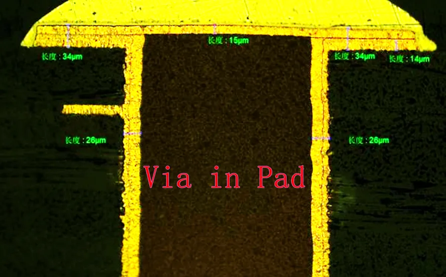
Filling methods distinguish via-in-pad from standard vias. Conductive filling, often copper electroplating, maintains low resistance and supports current carrying. Non-conductive epoxy fill prioritizes planarity and insulation, ideal for signal vias. Post-fill planarization via grinding or etching yields a flat copper cap over the via, preventing BGA ball collapse during reflow. This process aligns with high-reliability requirements, mitigating risks like outgassing or delamination. Engineers simulate thermal profiles to validate fill efficacy before tape-out.
Key Considerations for BGA Via Size and Structure
BGA via size directly influences fanout density and fabrication yield. Smaller diameters enable more vias per pad array but challenge aspect ratios and plating uniformity. Engineers select sizes where via diameter fits within 50-70% of the BGA pad, leaving adequate annular ring for solder fillet formation. Minimum drill sizes depend on laser or mechanical capabilities, with microvias suiting pitches below 0.4 mm. Oversized vias encroach on adjacent pads, complicating BGA escape routing. Balancing these factors optimizes via-in-pad BGA performance while adhering to design rules.
Annular ring requirements prevent via breakout and ensure plating coverage. IPC guidelines specify minimum rings based on via class and layer count, with tighter tolerances for HDI. For via-in-pad BGA, the effective pad expands to encompass the via, demanding precise mask and solder paste definition. Stackup thickness dictates feasible sizes; thicker boards necessitate larger drills to maintain aspect ratios under 8:1 or 10:1. Simulations predict impedance mismatches from via stubs, guiding size selection for high-speed signals.
Strategies for BGA Fanout and Escape Routing
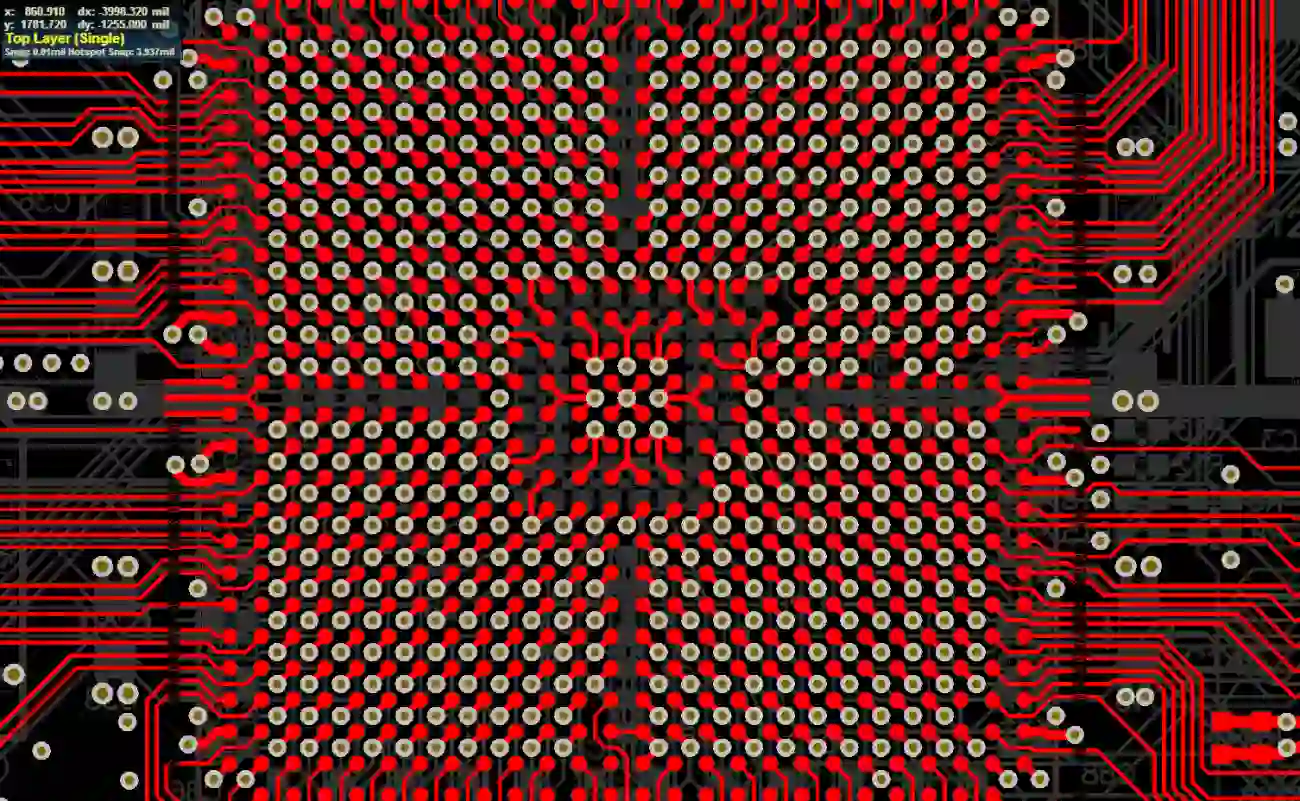
Effective BGA fanout patterns dictate trace escape from the perimeter to inner layers. Via-in-pad supports full-array fanout, routing every ball without peripheral dogbones. Staggered via grids across layers multiply channels, critical for 1000+ I/O BGAs. Trace widths and spaces scale with current density, often 3-4 mil for fine escape routing. Critical nets prioritize shortest paths to bypass capacitors. This structured approach resolves routing congestion in dense via-in-pad BGA designs.
Escape routing employs dogbone escapes for larger pitches, transitioning to via-in-pad for sub-0.5 mm. Multi-layer fanout uses blind vias stacking to L4-L6, preserving top layers for signals. Via staggering avoids drill alignment issues, enhancing yield. Length-matched routing for differential pairs follows via-in-pad paths to minimize skew. Engineers allocate escape zones during placement, verifying density with DRC tools.
BGA Soldering Challenges and Mitigation in Via-in-Pad Designs
BGA soldering via reflow demands filled vias to prevent molten solder wicking into barrels, which depletes joint volume and induces voids. Unfilled vias trap flux residues, compromising reliability under IPC Class 3 criteria. Conductive fills minimize thermal resistance during reflow peaks, while non-conductive options reduce voiding by blocking capillary action. Post-reflow inspection per J-STD-001 verifies joint fillet and void percentages below 25%. Profile optimization controls ramp rates to avoid via plug outgassing. These measures ensure via-in-pad BGA solder joints withstand vibration and temperature excursions.
Surface finishes like ENIG or OSP interact with via caps, influencing wettability. Planar caps prevent ball bridging, a common defect in dense arrays. X-ray and SAM inspections quantify voids correlated to fill quality. Rework challenges escalate with via-in-pad, necessitating site-specific BGA removal techniques.
Best Practices for Robust Via-in-Pad BGA Designs
Collaborate early with fabricators on via specs, confirming fill methods and aspect ratios. Simulate solder volume to predict joint standoff, integrating IPC-7095 land patterns. Employ thermal reliefs sparingly to balance heat dissipation without reflow inhibition. Validate stackups for via reliability under JEDEC thermal cycling. Document DFM checklists covering BGA via size, fanout layers, and escape trace rules. Iterative DRC and auto-routing refine via-in-pad BGA layouts for production readiness.
Layer budgeting prioritizes power/ground escapes first, followed by high-speed signals. Microvia clusters enhance density but cap at three levels per IPC guidelines. Cost modeling weighs fill premiums against layer reductions.
Conclusion
Via-in-pad design revolutionizes BGA integration, enabling unprecedented routing densities through optimized fanout and escape strategies. Critical focus on via sizing, filling, and soldering processes ensures mechanical and electrical reliability. Electric engineers benefit from structured adherence to standards like IPC-7095 and J-STD-001, mitigating risks in high-density PCBs. Proactive DFM and simulation yield robust assemblies. As pitches shrink, via-in-pad remains pivotal for next-generation electronics.
FAQs
Q1: What is via-in-pad BGA and when should electric engineers use it?
A1: Via-in-pad BGA places vias directly in BGA pads for fine-pitch components under 0.5 mm, essential for dense BGA fanout. Use it when dogbone escapes fail due to space constraints, prioritizing high I/O counts. It reduces inductance and supports multilayer routing. Coordinate with fabricators for fill processes to ensure planarity. This technique aligns with high-reliability needs per industry standards.
Q2: How does BGA via size impact escape routing?
A2: BGA via size determines annular ring and aspect ratio feasibility, directly affecting trace channel count in escape routing. Smaller sizes enable tighter via-in-pad BGA fanout but risk plating defects. Balance with pad diameter to maintain solder joint integrity. Fabricator capabilities guide minimums, often favoring microvias for pitches below 0.65 mm. Simulations verify impedance control.
Q3: What are best practices for BGA soldering with via-in-pad?
A3: Mandate via filling to prevent solder wicking, using conductive or non-conductive methods for planar caps. Optimize reflow profiles per J-STD-001 to limit voids under 25%. Select finishes enhancing wettability without residue. Post-assembly X-ray confirms joint quality. This ensures via-in-pad BGA reliability in thermal cycling.
Q4: Why is via filling critical for via-in-pad BGA fanout?
A4: Filling blocks solder migration during BGA soldering, preserving joint volume and minimizing voids. It provides planarity for uniform ball collapse and enhances thermal/electrical performance. Non-conductive fills insulate signals; conductive ones carry current. Unfilled vias compromise reliability, especially in dense fanout arrays. Always planarize for HDI compatibility.
References
IPC-7095 — Design and Assembly Process Implementation for Ball Grid Array (BGA). IPC
J-STD-001 — Requirements for Soldered Electrical and Electronic Assemblies. IPC/JEDEC
IPC-6012 — Qualification and Performance Specification for Rigid Printed Boards. IPC


