 ALLPCB


Introduction
Signal integrity medical imaging represents a critical aspect of PCB design, particularly in devices like MRI machines and CT scanners where precise signal transmission directly impacts diagnostic accuracy. In these high-stakes applications, even minor distortions in electrical signals can lead to image artifacts or false readings, compromising patient care. Engineers must address challenges such as high-frequency RF signals in MRI systems and gigabit data rates in CT detectors, ensuring signals maintain their shape, timing, and amplitude throughout the PCB. This article explores the causes of signal integrity issues, targeted design strategies for medical imaging PCBs, and proven troubleshooting methods. By focusing on controlled impedance and simulation techniques, designers can mitigate risks and achieve reliable performance. Understanding these principles enables electric engineers to optimize PCB layouts for demanding medical environments.
Understanding Signal Integrity in Medical Imaging PCBs
Signal integrity refers to the ability of an electrical signal to propagate from source to receiver without distortion, encompassing aspects like reflections, crosstalk, and attenuation. In medical imaging, PCBs handle ultra-high-speed data and sensitive analog signals, making signal integrity paramount for clear image reconstruction. For instance, MRI systems transmit RF pulses at frequencies exceeding 100 MHz, while CT scanners process detector signals at data rates over 10 Gbps. Poor signal integrity can introduce jitter or noise, degrading image quality and violating safety thresholds. Compliance with standards like IPC-2141 for controlled impedance ensures predictable signal behavior across varying operating conditions. Electric engineers prioritize these factors during the initial design phase to avoid costly iterations.
Common Causes of Signal Integrity Problems
Impedance mismatches top the list of signal integrity issues, occurring at vias, connectors, or trace transitions where the characteristic impedance deviates from the target value. Reflections arise when signals encounter these discontinuities, bouncing back and interfering with subsequent bits in high-speed links. Crosstalk becomes prevalent in dense layouts, with aggressor traces coupling noise into victim lines through capacitive or inductive mechanisms. Dielectric losses increase with frequency due to material absorption, particularly in thicker stackups common to medical PCBs. Environmental factors, such as strong magnetic fields in MRI machines, exacerbate electromagnetic interference, inducing unwanted voltages. Ground bounce and power supply noise further compound these effects, demanding robust power distribution networks.
PCB Design for MRI Machines: Key Considerations
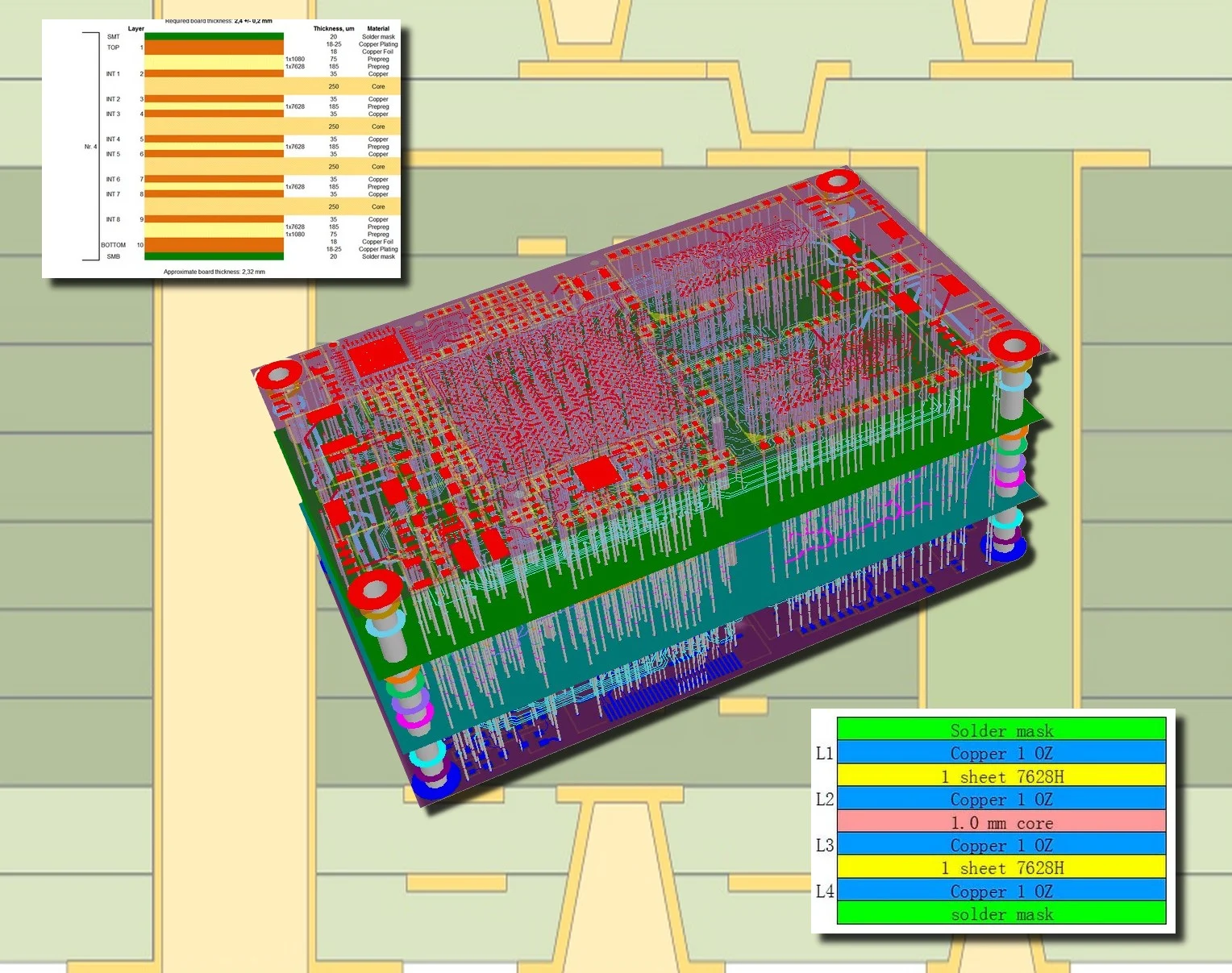
PCB design for MRI machines requires meticulous attention to RF signal paths, where gradient and RF coils demand low-loss transmission lines with precise controlled impedance. Stackups often feature symmetric layers to minimize warpage and maintain impedance stability under thermal stress. Shielding planes and guard traces isolate sensitive analog sections from digital noise sources. Length tuning compensates for propagation delays in multi-channel receiver coils, ensuring phase alignment. Vias must use back-drilling to eliminate stubs that cause resonances at MRI frequencies. Adhering to IPC-6012 performance specifications guarantees the mechanical integrity supports these electrical demands.
High magnetic fields necessitate non-magnetic materials and careful component selection to prevent induced currents. Differential routing for RF signals reduces common-mode noise pickup. Engineers simulate field interactions early to predict shielding effectiveness. Ground stitching vias along seams enhance return path integrity. These practices collectively preserve signal fidelity in the harsh MRI environment.
PCB Design for CT Scanners: High-Speed Data Challenges
PCB design for CT scanners focuses on gigabit serial links from detector arrays, where eye closure from jitter or inter-symbol interference poses significant risks. Multilayer stackups with embedded dielectrics achieve 100-ohm differential impedance with tight tolerances. Serpentine length matching equalizes skew across parallel data channels. Via farms and blind vias optimize density while minimizing stub effects. Power planes with decoupling capacitors suppress simultaneous switching noise. Signal integrity simulation medical PCB verifies these elements pre-fabrication.
Crosstalk mitigation involves wider spacing and orthogonal routing between layers. Reference planes provide continuous return paths, reducing radiation losses. Engineers target low insertion loss through low-Dk materials in signal layers. Decoupling strategies extend to on-board regulators for stable voltage rails. These targeted designs ensure CT scanners deliver artifact-free reconstructions.
The Role of Controlled Impedance in Medical Imaging PCBs
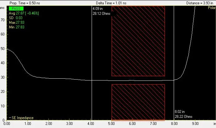
Controlled impedance PCB medical imaging forms the foundation for reliable high-speed performance, targeting tolerances like ±10% to match driver and receiver specifications. Characteristic impedance depends on trace width, thickness, dielectric height, and material properties, governed by transmission line equations. Microstrip and stripline configurations offer trade-offs in loss versus shielding. Fabrication processes must verify impedance via test coupons per IPC-2141 guidelines. Variations from etching tolerances or glass weave effects necessitate field solver corrections. Engineers iterate stackups to balance impedance, crosstalk, and manufacturability.
Signal Integrity Simulation for Medical PCBs
Signal integrity simulation medical PCB involves pre-layout modeling of S-parameters and eye diagrams to predict real-world behavior. Time-domain simulations capture reflections and jitter, while frequency-domain analysis reveals insertion and return loss. IBIS models for components enable system-level verification. Post-layout extraction accounts for actual routing geometries. Sensitivity analysis identifies critical parameters like via spacing. These simulations guide optimizations before prototyping.
HyperLynx or similar workflows validate differential pairs and clock trees. Monte Carlo runs assess process variations. Correlation with measurements refines models iteratively. For medical applications, simulations include EMI coupling from external fields. This proactive approach minimizes respins and accelerates time-to-market.
Troubleshooting Signal Integrity Issues: Step-by-Step Approach
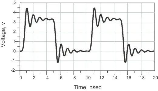
Begin troubleshooting with time-domain reflectometry (TDR) to map impedance profiles along traces. Oscilloscopes capture eye patterns, quantifying jitter and margin. Vector network analyzers measure S-parameters for loss and crosstalk. Isolate issues by de-embedding fixtures and probing intermediates. Thermal cycling reveals temperature-dependent drifts. Correlate findings with simulations to pinpoint root causes.
For MRI-specific problems, Faraday cage tests simulate magnetic interference. CT troubleshooting emphasizes bit error rate testing under load. Fabric defects like plating voids show as high-resistance discontinuities. Documentation of measurements supports design reviews. Iterative fixes, such as rerouting or adding shielding, resolve most issues.
Best Practices for Prevention and Optimization
Implement full ground planes under high-speed signals to stabilize reference impedance. Use differential pairs with tight length matching and constant spacing. Minimize via count through fanouts and blind/buried preferences. Decouple aggressively at IC pins with low-ESL capacitors. Route critical nets first on inner layers. Verify with flying probe impedance testing post-fabrication.
Layer sequencing alternates signal and plane for coupling. Orthogonal routing reduces broadside crosstalk. Bevel connectors for smooth transitions. Maintain consistent dielectric thickness. These practices, aligned with IPC standards, yield robust medical imaging PCBs.
Conclusion
Troubleshooting signal integrity issues in medical imaging PCBs demands a holistic approach from design through verification. Key strategies include controlled impedance, targeted simulations, and rigorous measurements tailored to MRI and CT requirements. By addressing reflections, crosstalk, and EMI proactively, engineers ensure diagnostic precision and patient safety. Standards like IPC-2141 and IEC 60601 provide essential frameworks for compliance. Implementing these best practices reduces risks and enhances PCB reliability. Electric engineers equipped with these insights can deliver high-performance solutions for advancing medical technology.
FAQs
Q1: What is signal integrity medical imaging, and why does it matter for PCBs?
A1: Signal integrity medical imaging ensures electrical signals in PCBs remain undistorted during transmission, crucial for accurate image data in MRI and CT systems. Distortions like jitter or noise can cause artifacts, leading to misdiagnoses. Engineers achieve this through controlled impedance traces and shielding. Simulations predict issues early. Compliance with IPC guidelines maintains quality. This focus directly supports reliable diagnostics.
Q2: How does PCB design for MRI machines address signal integrity challenges?
A2: PCB design for MRI machines incorporates RF-optimized stackups with symmetric layers for impedance control and low loss. Shielding isolates signals from magnetic fields, while back-drilled vias eliminate resonances. Differential routing minimizes noise pickup. Simulations verify phase alignment across coils. Ground stitching enhances return paths. These measures preserve microvolt-level signals essential for imaging fidelity.
Q3: What role does signal integrity simulation play in medical PCB development?
A3: Signal integrity simulation medical PCB models reflections, crosstalk, and jitter using S-parameters and eye diagrams. Pre-layout runs guide routing, while post-layout verifies fabrication. Sensitivity to process variations informs tolerances. It reduces prototyping costs by identifying fixes early. For CT scanners, it ensures gigabit links meet BER targets. This step is vital for high-reliability medical applications.
Q4: Why is controlled impedance critical in medical imaging PCBs?
A4: Controlled impedance PCB medical imaging prevents mismatches that cause reflections and signal degradation in high-speed paths. Targeting ±10% tolerance matches driver-receiver specs, per IPC-2141. Stackup design balances width, height, and dielectric. Test coupons confirm fabrication accuracy. It mitigates losses in MRI RF and CT data lines. Consistent impedance ensures diagnostic precision.
References
IPC-2141A - Design Guide for High Speed Controlled Impedance Circuit Boards. IPC
IPC-6012E - Qualification and Performance Specification for Rigid Printed Boards. IPC, 2015
IEC 60601-1 - Medical electrical equipment - Part 1: General requirements for basic safety and essential performance. IEC, 2005
IPC-2221G - Generic Standard on Printed Board Design. IPC, 2023


