 ALLPCB


Molded Interconnect Device (MID) PCBs combine injection-molded plastic substrates with integrated conductive circuits, enabling compact three-dimensional electronic assemblies. These components find use in automotive sensors, medical devices, and consumer electronics where space constraints demand complex geometries. Manufacturing defects in MID PCBs can compromise electrical performance, mechanical integrity, and long-term reliability. Engineers and quality teams therefore focus on systematic identification and correction of issues that arise during molding, laser structuring, and plating stages. Effective troubleshooting supports consistent production yields and meets the expectations of high-reliability applications.
What Are MID PCBs and Why Defect Troubleshooting Matters
MID technology integrates mechanical and electrical functions into a single molded part, reducing assembly steps compared with traditional rigid or flexible printed circuit boards. The process typically involves laser direct structuring (LDS) to create circuit patterns on the molded surface, followed by selective plating. Defects introduced at any stage affect via continuity, trace adhesion, and overall dimensional stability. Quality control MID PCB practices emphasize early detection because rework on three-dimensional structures proves costly and technically challenging. Factory teams apply standardized inspection protocols to maintain process capability and minimize scrap rates across production runs.
Technical Principles and Common Causes of Defects
Molding defects MID originate from thermal and mechanical stresses during injection molding. Uneven cooling rates produce warpage or sink marks that distort the substrate geometry and misalign subsequent laser patterns. Voids or delamination within the plastic can create weak points that propagate under thermal cycling. These substrate imperfections directly influence the accuracy of laser ablation and the uniformity of subsequent metal deposition.

LDS plating issues frequently stem from surface activation inconsistencies or contamination. Incomplete laser activation leaves areas without catalytic seeds, resulting in patchy copper growth or open circuits. Over-plating or excessive thickness variations occur when bath chemistry drifts outside controlled parameters, leading to bridging between adjacent traces. Poor adhesion between the plated metal and the polymer substrate manifests as peeling or blistering during reflow or mechanical handling.
Related Reading: The Benefits of Laser Direct Structuring (LDS) in Rigid Flex PCB Assembly
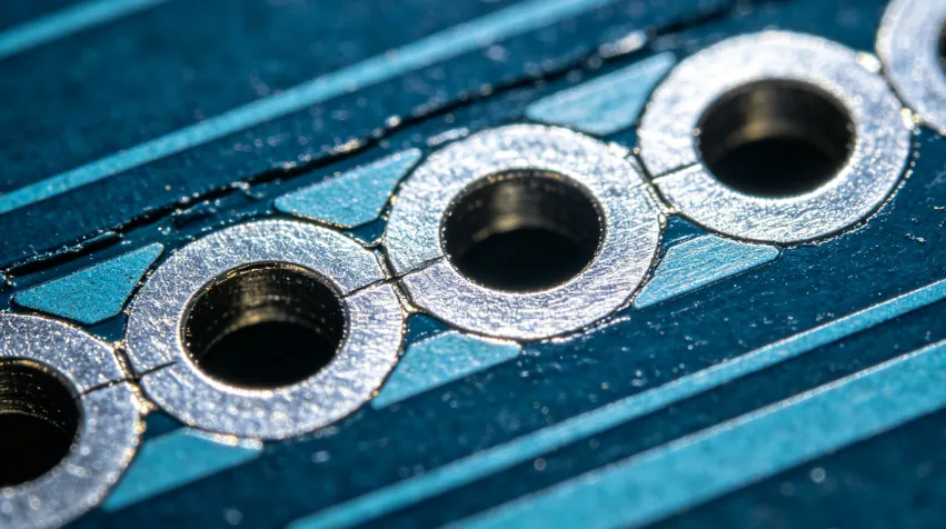
Via failures MID arise when through-holes or z-axis connections formed during molding or drilling do not receive adequate plating coverage. Insufficient copper thickness inside vias increases resistance and creates thermal hotspots. Misalignment between molded features and laser-drilled vias further reduces contact area and elevates the risk of intermittent opens. These failures become evident during electrical testing or after environmental stress.
Practical Solutions and Best Practices
Process optimization begins with tight control of molding parameters, including melt temperature, injection speed, and cooling time, to minimize substrate distortion. Regular mold maintenance and use of balanced runner systems help achieve uniform filling and reduce internal stresses. Post-molding annealing steps can relieve residual stresses before laser structuring.
For LDS plating issues, factories maintain strict bath chemistry monitoring and implement automated laser power calibration routines. Surface cleaning protocols prior to activation remove mold release agents and contaminants that interfere with plating initiation. Inline optical inspection after laser structuring verifies pattern fidelity before plating begins.
Via quality improves through optimized drilling parameters and controlled electroless and electrolytic plating sequences. Current density profiling during electroplating ensures even deposition inside high-aspect-ratio features. Electrical continuity testing combined with cross-sectional analysis confirms via integrity before final assembly.
Quality control MID PCB programs incorporate statistical process control at each stage. Sampling plans aligned with acceptance criteria detect trends before defects reach critical levels. When deviations appear, root-cause analysis using fishbone diagrams or failure mode analysis guides corrective actions. These disciplined approaches reduce defect rates while preserving throughput.
Related Reading: Tackling Challenging Geometries: Solder Paste Dispensing on 3D MIDs
Conclusion
Systematic troubleshooting of MID PCB manufacturing defects requires coordinated control of molding, laser structuring, and plating operations. Attention to substrate geometry, surface activation, and plating uniformity prevents the most common failure modes. Adherence to established industry standards supports repeatable quality outcomes across production lots. Engineers who apply these factory-driven methods achieve higher yields and greater confidence in the reliability of three-dimensional electronic assemblies.
FAQs
Q1: What are the most frequent MID PCB manufacturing defects encountered in production?
A1: Molding defects MID such as warpage and sink marks, LDS plating issues including incomplete coverage and poor adhesion, and via failures MID caused by insufficient plating thickness represent the primary concerns. These issues arise from process variations in temperature, laser parameters, and bath chemistry. Early detection through standardized inspection reduces their impact on final product performance.
Q2: How do LDS plating issues affect MID PCB reliability?
A2: LDS plating issues create non-uniform conductor thickness or weak metal-to-polymer bonds that lead to electrical opens or mechanical delamination under thermal or mechanical stress. Consistent bath control and surface preparation minimize these risks. Resulting defects compromise signal integrity and long-term durability in demanding applications.
Q3: What role does quality control play in preventing via failures MID?
A3: Quality control MID PCB activities include dimensional verification of molded features, laser pattern inspection, and electrical testing of plated vias. Cross-sectional analysis verifies plating thickness and coverage. These steps ensure via continuity meets design requirements before boards proceed to assembly.
Q4: Which industry standards guide MID PCB defect prevention?
A4: IPC-6012E provides qualification and performance requirements applicable to the rigid aspects of MID constructions. IPC-A-600K defines acceptability criteria for printed board features, including plated vias and surface finishes. ISO 9001:2015 establishes the quality management framework that supports consistent process control throughout MID manufacturing.
References
IPC-6012E — Qualification and Performance Specification for Rigid Printed Boards. IPC, 2017
IPC-A-600K — Acceptability of Printed Boards. IPC, 2020
ISO 9001:2015 — Quality Management Systems. ISO, 2015





