ALLPCB


What Are 14-Layer PCB Manufacturing Defects and Why They Matter
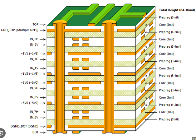
A 14-layer PCB consists of multiple copper and dielectric layers laminated under heat and pressure, creating a rigid structure with high interconnect density. Manufacturing defects in such boards include warpage, delamination, via plating voids, inner-layer registration errors, and soldering anomalies during assembly. These issues arise from the interaction of materials, processes, and thermal profiles inherent to multilayer fabrication.
Defects in 14-layer PCBs matter because they can cause electrical opens, shorts, or intermittent failures that compromise entire assemblies. In sectors such as telecommunications, aerospace, and industrial controls, even minor deviations may lead to costly rework or field returns. Compliance with established quality frameworks helps manufacturers identify and mitigate risks early in production.
Technical Principles and Mechanisms Behind Common Defects
Warpage occurs when residual stresses from lamination and subsequent thermal excursions cause the board to bend or twist. Coefficient of thermal expansion mismatches between copper, resin systems, and glass reinforcements contribute to this distortion, particularly in boards with asymmetric copper distribution across the 14 layers. Uneven cooling rates after pressing can further exacerbate the condition.
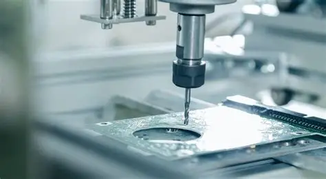
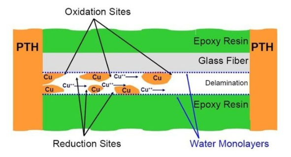
Delamination results from inadequate resin flow or moisture entrapment during lamination, creating voids between layers that propagate under thermal or mechanical stress. Via defects, such as plating voids or barrel cracks, stem from incomplete electroless or electrolytic copper deposition inside high-aspect-ratio holes drilled through the stack-up. These voids reduce current-carrying capacity and create stress concentration points.
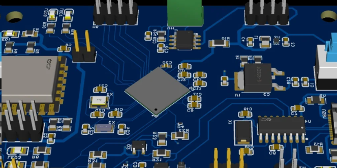
Soldering problems during assembly, including bridges, opens, or insufficient wetting, often trace back to surface finish inconsistencies or solder mask registration errors on the outer layers. Inner-layer misalignment during imaging and etching compounds via-to-pad registration issues, increasing the likelihood of open circuits in buried or blind vias. Process variables such as press temperature profiles, drill parameters, and desmear chemistry directly influence defect formation rates.
Inspection Techniques and Troubleshooting Approaches
Visual and automated optical inspection provides the first line of defense for surface-level defects such as solder mask misalignment or outer-layer copper anomalies. For internal features, X-ray imaging and acoustic microscopy detect delamination and via plating issues without destroying the board. Cross-sectional analysis remains the definitive method for confirming plating thickness and void presence in critical vias.
When warpage exceeds acceptable limits, engineers measure bow and twist using standardized fixtures and compare results against board thickness and size. Root-cause analysis typically involves reviewing lamination press records, material lot data, and copper balance calculations. For via-related defects, adjusting drill feed rates, improving hole cleaning sequences, or modifying plating current densities often resolves the issue in subsequent production runs.
Soldering defects identified during assembly require evaluation of stencil design, reflow profiles, and component placement accuracy. Process adjustments such as optimizing peak temperature and time above liquidus help achieve consistent wetting while avoiding excessive intermetallic growth. Documentation of each defect type, location, and corrective action supports continuous improvement in multilayer production.
Best Practices for Prevention and Quality Control
Maintaining tight control over material selection and incoming inspection reduces variability that leads to defects. Symmetric copper distribution and balanced dielectric thicknesses across the 14 layers minimize warpage potential. Strict adherence to lamination parameters, including controlled heating and cooling ramps, helps achieve void-free bonding between layers.
Via formation benefits from validated drill and plating processes, with regular monitoring of hole wall quality through microsectioning. Implementing design rules that account for minimum annular ring and aspect ratio limits supports reliable plating. During assembly, consistent surface finish application and precise solder mask alignment prevent many soldering issues.
Quality systems aligned with industry standards provide the framework for systematic defect prevention. Regular audits of process capability and failure mode analysis enable proactive adjustments before defects reach final inspection.
Conclusion
Effective troubleshooting of 14-layer PCB manufacturing defects requires understanding the interplay between design, materials, and process parameters. Structured inspection combined with root-cause analysis allows manufacturers to address warpage, delamination, via plating issues, and soldering problems at their source. Consistent application of proven controls and adherence to recognized quality specifications supports higher yields and reliable performance in complex electronic systems.
FAQs
Q1: What are the most common 14-layer PCB manufacturing defects encountered during production?
A1: Warpage, delamination, via plating voids, and inner-layer registration errors represent frequent challenges in 14-layer PCB manufacturing. These defects arise from thermal stresses, material interactions, and process variations during lamination and plating. Early detection through appropriate inspection methods helps limit their impact on assembly yield.
Q2: How do via defects affect the reliability of multilayer PCBs?
A2: Via defects such as plating voids or barrel cracks reduce the electrical continuity and mechanical strength of interconnections in multilayer boards. They can lead to increased resistance, heat generation, or eventual open circuits under operational stress. Proper process controls during drilling and copper deposition minimize these risks in 14-layer constructions.
Q3: What role do industry standards play in addressing PCB assembly issues?
A3: Standards such as IPC-A-600K establish visual and dimensional acceptance criteria that guide inspection of printed boards, including multilayer types. J-STD-001 provides requirements for soldering processes that help prevent common assembly defects. Following these frameworks supports consistent quality across production batches.
Q4: Why is warpage a particular concern for 14-layer PCBs?
A4: The increased number of layers and copper planes in 14-layer designs amplifies the effects of thermal expansion mismatches during fabrication and assembly. Excessive warpage can cause component placement errors, poor solder joint formation, or difficulties in subsequent handling and testing. Controlled lamination and balanced stack-up designs help manage this issue.
References
IPC-6012E - Qualification and Performance Specification for Rigid Printed Boards. IPC, 2017
IPC-A-600K - Acceptability of Printed Boards. IPC, 2020
J-STD-001H - Requirements for Soldered Electrical and Electronic Assemblies. IPC, 2020
IPC-A-610H - Acceptability of Electronic Assemblies. IPC, 2020