 ALLPCB


Introduction
Power supply PCBs form the backbone of any electronic project, converting raw AC or DC input into stable voltages that devices need to operate reliably. For electronic hobbyists, mastering power supply PCB basics opens the door to building everything from simple LED drivers to custom amplifiers without relying on off-the-shelf modules. These boards handle critical tasks like voltage regulation, noise filtering, and current delivery, making them a foundational skill in electronics. Understanding power supply PCB components explained in detail helps avoid common pitfalls such as overheating or instability that can ruin projects. This guide provides a step-by-step power supply PCB design process tailored for beginners, drawing on logical engineering principles to ensure your designs work the first time. By the end, you will have the confidence to create robust power supplies for your hobby setups.
Power Supply PCB Basics
A power supply PCB is a printed circuit board that integrates components to manage electrical power distribution efficiently. It takes an input source, such as wall AC or a battery, and outputs clean, regulated DC power at desired levels for connected circuits. In hobbyist projects, these PCBs ensure devices run smoothly without voltage drops or electrical noise interfering with signals. Key aspects include input protection, conversion stages, and output filtering, all arranged to minimize losses and heat. Power supply PCB basics revolve around balancing efficiency, size, and cost, which directly impacts project performance. For beginners, starting with low-power designs under 5 amps keeps complexity manageable while teaching core concepts.
The relevance of power supply PCBs cannot be overstated in the hobbyist world. Unstable power often causes erratic behavior in microcontrollers or audio circuits, leading to frustrating debugging sessions. A well-designed board provides consistent voltage, protecting sensitive components from damage. It also allows customization, like adding multiple outputs for different project needs. Industry standards like IPC-2221B guide these designs by outlining spacing and trace width requirements for safe operation. Mastering these basics empowers hobbyists to prototype reliably and scale up to more ambitious builds.
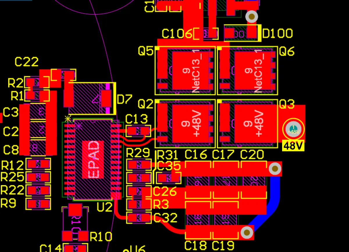
Key Power Supply PCB Components Explained
Power supply PCB components explained start with the input stage, where fuses or resistors protect against surges. Rectifier diodes or bridges convert AC to pulsating DC, essential for AC-powered supplies. Smoothing capacitors follow, storing charge to reduce ripple and provide steady current. Voltage regulators, either linear like 78xx series or switching ICs, maintain output stability despite load changes. Inductors and additional capacitors form filters in switching designs to handle high frequencies.
Output components include electrolytic capacitors for bulk storage and ceramic ones for high-frequency noise suppression. Heat sinks or thermal pads manage dissipation from regulators and passives. Control ICs oversee feedback loops, ensuring precise voltage. Each part must match ratings for voltage, current, and temperature to prevent failures. Proper selection based on power supply PCB components explained ensures longevity and efficiency in hobby projects.
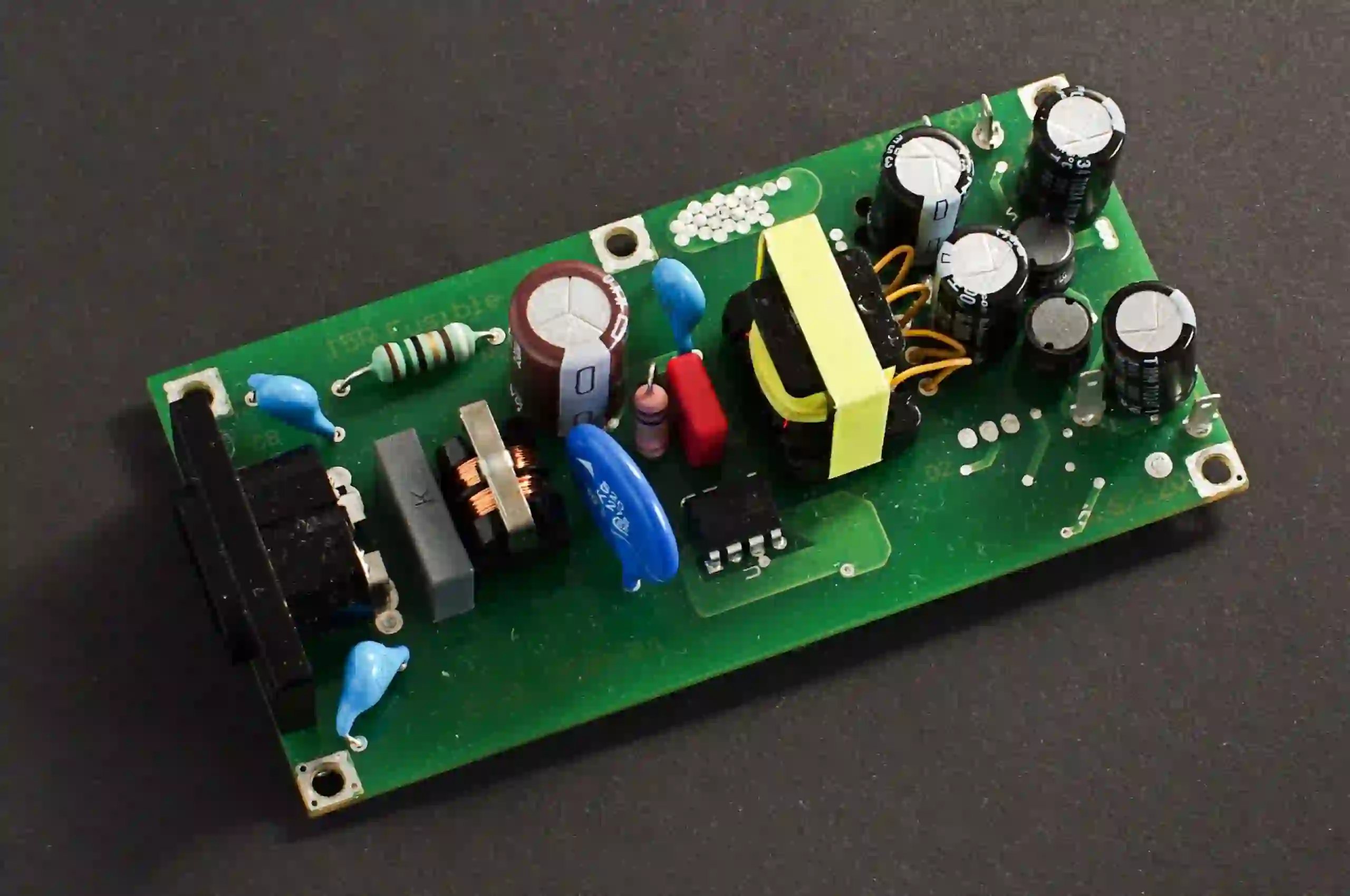
Transformers or inductors step down voltage in linear supplies, while MOSFETs switch rapidly in buck converters. Feedback resistors set output levels accurately. PCB mounting hardware secures heavy parts against vibration. Understanding interactions, like capacitor ESR affecting stability, is crucial. Hobbyists benefit from through-hole parts initially for easy prototyping before surface-mount transitions.
Understanding Power Supply Topologies for PCB Design
Power supply topologies define how energy converts on the PCB, with linear and switching as primary types. Linear supplies use simple drop-out regulation, ideal for low-noise audio hobby projects due to minimal ripple. They dissipate excess power as heat, suiting low-current applications under 1 amp. Switching topologies, like buck or boost, achieve high efficiency above 80 percent by pulsing energy through inductors. These suit battery-powered gadgets but introduce EMI challenges requiring careful layout.
The choice impacts PCB real estate and component count. Linear designs need larger heat sinks, while switching demands tight trace routing for high currents. Feedback loops in both maintain regulation, but switching uses optocouplers for isolation. Hobbyists often start with linear for simplicity, progressing to switching for portable builds. J-STD-001ES provides soldering guidelines for these mixed-technology boards. Each topology's principles guide component placement to optimize performance.
Step-by-Step Power Supply PCB Design
Step-by-step power supply PCB design begins with defining requirements: input voltage range, output specs, and max load. Sketch a schematic capturing the topology, placing regulators centrally with input protection first. Select components with margins, like 20 percent above rated current, and note footprints. Simulate mentally or note key values like ripple targets under 50mV. This phase ensures feasibility before layout.
Next, create the PCB layout starting with a two-layer board for simplicity. Position high-current paths from input to output with wide traces, following IPC-2221B current capacity charts. Place decoupling capacitors close to IC pins, within 0.5 inches. Route ground planes solidly under noise-sensitive areas. Add vias for thermal relief on pads.
Third, focus on power supply PCB routing: separate analog and digital grounds, star-pointing at the regulator. Minimize loop areas for switching traces to cut EMI. Use silk screens for polarity and values. Fourth, incorporate safety: creepage distances per standards, fuse holders, and silkscreen warnings. Generate Gerber files after DRC checks.
Finally, review for manufacturability: via sizes over 0.3mm, no acute angles. Prototype on perfboard first to validate. Iterate based on bench tests for voltage stability and heat. This methodical approach builds reliable power supply PCB designs for hobbyists.
Best Practices for Power Supply PCB Layout and Fabrication
Effective power supply PCB layout prioritizes thermal management with vias under hot components and copper pours for heat spreading. Decoupling uses multiple cap values in parallel for broad frequency coverage. Ground planes shield signals, poured on inner layers if multilayer. Keep high dv/dt traces short and away from outputs. These practices reduce noise coupling significantly.
Component orientation aids assembly: align polarities, group by function. Use 45-degree bends on traces for signal integrity. For hobbyists, FR4 material suffices with 1oz copper for currents up to 2 amps. Solder mask over pads prevents shorts. Post-layout, verify trace widths exceed minimums per current.
EMI mitigation involves ferrite beads on inputs and snubbers across switches. Test for compliance with scopes on ripple. Standards like IPC-A-610H define acceptability for soldered joints. Document revisions for future tweaks. These best practices elevate hobby projects to professional levels.
Common Pitfalls and Troubleshooting in Power Supply PCBs
Overlooking trace resistance causes voltage drops under load, fixed by thicker copper. Poor grounding induces hum, resolved by single-point returns. Overheating signals inadequate cooling, addressed with fans or larger sinks. Oscillation from insufficient bypassing needs extra ceramics. Measure with multimeters and scopes step-by-step.
Ripple exceeding specs points to small caps; upgrade capacitance. Startup issues stem from inrush, mitigated by NTC thermistors. Systematic checks post-assembly save time. Learning these turns failures into skills.
Conclusion
Power supply PCB design blends basics, components, and structured steps into reliable hobbyist projects. From understanding topologies to layout best practices, each element ensures stable power delivery. Reference standards like IPC-2221B and J-STD-001ES anchor designs in proven methods. Hobbyists gain versatility for endless applications. Start simple, test thoroughly, and iterate to perfection.
FAQs
Q1: What are the power supply PCB basics every hobbyist should know?
A1: Power supply PCB basics include input protection, rectification, regulation, and filtering stages. These convert and stabilize power for circuits. Key is matching components to load needs while managing heat. Follow wide traces and decoupling for reliability. This foundation prevents common issues like instability.
Q2: How do power supply PCB components explained impact design choices?
A2: Power supply PCB components explained reveal roles: diodes rectify, capacitors smooth, regulators stabilize. Selection depends on efficiency and noise goals, like linear for quiet or switching for compact. Margins on ratings ensure safety. Proper placement minimizes interactions.
Q3: What is a step-by-step power supply PCB design process for beginners?
A3: Step-by-step power supply PCB design starts with specs and schematic, then component selection, layout, routing, and review. Route power paths wide, place decoupling close, and keep grounds solid. Prototype and test for ripple and heat. This logical flow builds working boards quickly.
Q4: Why follow standards in power supply PCB design?
A4: Standards like IPC-2221B ensure trace sizing and spacing for safety. They guide thermal and electrical integrity. Hobbyists avoid failures by adhering, gaining professional results. Consistent application scales projects reliably.


