 ALLPCB


Introduction
In electronic assembly inspection, precise component placement forms the foundation of reliable PCB performance. IPC-A-610 component placement criteria provide clear visual standards to evaluate alignment, orientation, and seating during visual inspection checklists. Engineers rely on these guidelines to identify defects early, ensuring assemblies meet quality expectations across applications from consumer devices to high-reliability systems. This article delivers a comprehensive visual inspection checklist tailored for PCB component alignment and SMT placement guidelines. By following these steps, teams can troubleshoot common issues and uphold electronic assembly inspection standards effectively. Mastering these practices reduces rework and enhances overall yield.
What Is IPC-A-610 Component Placement Inspection and Why It Matters
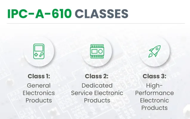
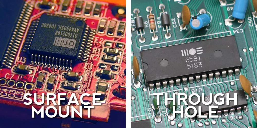
IPC-A-610 defines acceptability criteria for electronic assemblies, with specific sections addressing component placement in both surface-mount technology (SMT) and through-hole technology (THT). This standard categorizes assemblies into three classes based on end-use reliability needs: Class 1 for general electronics, Class 2 for dedicated service products, and Class 3 for high-performance applications. Component placement inspection verifies that parts are positioned correctly relative to pads or holes, preventing electrical shorts, mechanical stress, or soldering failures. Poor placement leads to issues like tombstoning in SMT or lead stress in THT, compromising signal integrity and thermal management. Adhering to these visual inspection checklists ensures compliance and longevity, particularly in demanding environments. Ultimately, IPC-A-610 component placement rules bridge design intent with manufacturing reality, minimizing field failures.
Key Technical Principles of Component Placement in IPC-A-610
Component placement principles in IPC-A-610 emphasize alignment, where components must center on designated lands or holes to support proper solder joint formation. For SMT parts, flat seating and minimal offset prevent uneven reflow, while THT requires leads to insert fully without bending or protrusion beyond specified limits. Class differences dictate tolerance levels: Class 2 permits minor visual offsets if functionality remains intact, whereas Class 3 demands precise positioning with no allowances for misalignment. Orientation verification is critical, especially for polarized components like diodes or capacitors, to avoid reverse polarity damage. Spacing between adjacent parts maintains electrical clearance and facilitates rework. These mechanisms ensure mechanical stability and electrical performance under vibration or thermal cycling.
In SMT assemblies, coplanarity of leads or terminations to the board surface is essential for uniform wetting during reflow soldering. Excessive tilt or standoff indicates placement errors from feeder issues or board warpage. THT placement focuses on lead clinch angles and protrusion lengths to secure components pre-soldering without stressing vias. IPC-A-610 outlines these as visual defects if they deviate from assembly documentation. Understanding class-specific thresholds helps inspectors prioritize high-risk areas. Proper placement directly influences downstream processes like automated optical inspection.
The Ultimate Visual Inspection Checklist for IPC-A-610 Component Placement
Use this structured visual inspection checklist to systematically evaluate PCB component alignment during electronic assembly inspection. Inspect under adequate magnification, typically 10x for fine-pitch parts, with consistent lighting to reveal shadows or gaps. Reference assembly drawings for orientation and position tolerances. Document defects with photos for root cause analysis. Proceed section by section for thorough coverage.
Orientation and Polarity
- Confirm all polarized components, such as diodes, LEDs, and electrolytic capacitors, match the silkscreen markings and documentation.
- Check ICs and connectors for correct pin one indicators or beveled edges.
- Verify no rotated parts exceeding allowable angles, which could cause functional failures.
- For Class 3, ensure zero tolerance for misorientation regardless of electrical test passage.
Alignment and Centering
- Measure offset from pad centerlines; Class 2 allows slight deviations if solder joints form properly, but Class 3 rejects any visible misalignment.
- Ensure terminations overlap pads adequately without excessive overhang that risks bridging.
- Inspect for consistent row alignment in arrays like BGAs or QFPs.
- Flag tombstoned chips where one end lifts due to uneven reflow.
Seating and Coplanarity
- Verify SMT components sit flat with no standoff greater than specification, indicating vacuum pickup errors.
- For THT, confirm leads protrude uniformly through holes without bending or splaying.
- Check for tilted parts that may shift during soldering.
- Use oblique lighting to detect subtle gaps under bodies.
Spacing and Clearance
- Measure gaps between adjacent components to prevent solder bridging or arcing.
- Ensure minimum distances per design rules, especially near high-voltage areas.
- Inspect for interference with fiducials or test points.
- Class 3 requires stricter clearances for thermal expansion reliability.
Damage and Integrity
- Scan for chipped bodies, bent leads, or cracked terminations from handling.
- Verify no pad lifts or tears from insertion force.
- Check markings legibility for traceability.
- Exclude assemblies with foreign objects under components.

This checklist aligns with SMT placement guidelines and supports 100% inspection for critical lots.
Best Practices for IPC-A-610 Compliant Visual Inspection
Implement standardized inspection stations with ESD-safe magnification and shadow-free illumination to optimize detection. Train operators on class distinctions to avoid over-rejection in Class 2 assemblies. Integrate automated optical inspection pre-manual review for high-volume runs, focusing human checks on exceptions. Maintain clean workspaces to prevent contamination mimicking placement defects. Calibrate placement machines regularly to minimize offsets at the source. Cross-reference with electrical testing, as visual passes do not guarantee functionality alone.
For troubleshooting, correlate defects to process steps: feeder jams cause misalignment, while paste volume issues lead to tombstoning. Adjust reflow profiles for better wetting on offset parts. Use fiducial marks for machine alignment verification. Document trends to refine stencil design or board supports. These practices elevate electronic assembly inspection efficiency.
Troubleshooting Common Component Placement Defects
Misalignment often stems from inaccurate pick-and-place programming or worn nozzles, resulting in shifted SMT parts. Inspectors spot this via uneven pad coverage; rework by reflowing with flux if within Class 2 limits. Tombstoning arises from rapid heating differentials, lifting small chips; mitigate with symmetric paste deposits and profiled ovens. THT lead bends indicate improper forming tools; straighten manually only if undamaged. Polarity errors from flipped trays demand barcode verification protocols. Excessive overhang in fine-pitch QFNs risks bridging; trim stencils for precise volume.
Board warpage exacerbates seating issues, detectable by rocking components; use fixtures during placement. For Class 3, even minor tilts fail due to vibration sensitivity. Root cause analysis via SPC charts identifies systemic problems. Quick fixes like hand-placement suit prototypes, but scale prevention through DOE. These insights make visual inspection checklists proactive tools.
Conclusion
IPC-A-610 component placement inspection ensures PCB assemblies withstand real-world stresses through rigorous visual checks. This ultimate checklist covers alignment, orientation, and more, adapting to class requirements for optimal results. Engineers applying these SMT placement guidelines reduce defects and boost reliability. Integrate best practices and troubleshooting to streamline workflows. Prioritizing these standards delivers high-quality electronic assemblies consistently.
FAQs
Q1: What are the main differences in IPC-A-610 component placement for Class 2 versus Class 3?
A1: Class 2 allows minor offsets and overhangs if electrical and mechanical performance holds, suiting dedicated service electronics. Class 3 enforces zero tolerance for misalignment or visual defects, critical for high-reliability uses like aerospace. Visual inspection checklists must adapt magnification and criteria accordingly. This distinction prevents over-specification in moderate applications while upholding stringent needs.
Q2: How do you check PCB component alignment during visual inspection?
A2: Examine centering on pads using rulers or software overlays against fiducials, ensuring overlaps meet IPC-A-610 thresholds. Oblique angles reveal offsets or tilts missed in top-down views. For SMT, confirm no more than allowable side overhang per class. Troubleshoot shifts by verifying machine calibration. Consistent checks maintain electronic assembly inspection integrity.
Q3: What causes common SMT placement defects in IPC-A-610 inspections?
A3: Feeder errors, paste inconsistencies, or reflow imbalances lead to misalignment and tombstoning. Warped boards hinder flat seating, while poor vacuum causes tilts. Visual checklists spot these via shadows or gaps. Address through process tuning and operator training for reliable PCB component alignment.
Q4: Why is orientation critical in IPC-A-610 visual inspection checklists?
A4: Incorrect polarity on diodes or capacitors causes immediate failures post-assembly. IPC-A-610 mandates matching silkscreen and documentation, especially for Class 3. Inspectors verify markings under magnification to catch flips. This step safeguards functionality in electronic assembly inspection routines.
References
IPC-A-610J - Acceptability of Electronic Assemblies. IPC, 2024
J-STD-001H - Requirements for Soldered Electrical and Electronic Assemblies. IPC, 2018


