 ALLPCB


Introduction
High-frequency PCB design presents unique challenges due to the shortened wavelengths of signals that behave more like transmission lines than simple conductors. Engineers must account for effects such as reflections, crosstalk, and radiation that degrade performance at frequencies where trace lengths approach a significant fraction of the signal wavelength. Simulation plays a pivotal role by allowing designers to predict and mitigate these issues early in the process, reducing iterations and costly prototypes. This guide explores the practical application of simulation in high-frequency PCB design, focusing on key areas like signal integrity, impedance control, and electromagnetic interference. By leveraging high-frequency PCB simulation tools within PCB design software simulation environments, engineers can achieve reliable designs that meet performance requirements. Understanding these techniques ensures robust operation in applications ranging from telecommunications to radar systems.
Challenges in High-Frequency PCB Design
At high frequencies, signals propagate along PCB traces with speeds determined by the dielectric properties of the materials, leading to potential mismatches if not properly managed. Parasitic effects from vias, bends, and discontinuities introduce losses and distortions that standard low-frequency design rules cannot address. Crosstalk between adjacent traces becomes prominent as capacitive and inductive coupling intensifies with frequency. Additionally, unintended radiation from traces can couple to nearby circuits or radiate externally, complicating compliance with electromagnetic compatibility requirements. These challenges demand a shift from empirical design to predictive modeling. Simulation addresses this by quantifying these effects before fabrication.
Why Simulation Matters in High-Frequency Design
Simulation enables engineers to virtualize the PCB environment, analyzing how signals interact with the physical layout without building hardware. It reveals issues like eye diagram closure or excessive jitter that might only appear during testing. By iterating designs digitally, teams save time and resources while improving yield. High-frequency PCB simulation tools integrate seamlessly into the design flow, providing insights into material selection, stackup optimization, and routing strategies. This approach aligns with industry practices outlined in standards like IPC-2221C, which emphasizes design requirements for reliable performance. Ultimately, simulation bridges the gap between schematic intent and physical realization.
Key Principles of High-Frequency Signal Propagation
Signal propagation in high-frequency PCBs follows transmission line theory, where characteristic impedance governs reflection coefficients at discontinuities. The skin effect confines current to the conductor surface, increasing resistance and losses as frequency rises. Dielectric losses from the substrate material further attenuate signals, necessitating low-loss laminates. Vias act as impedance bumps, causing return path disruptions if not stubbed or back-drilled appropriately. Engineers must model these using field solvers within PCB design software simulation to predict S-parameters accurately. Proper understanding of these principles forms the foundation for effective simulation strategies.
Signal Integrity Simulation
Signal integrity simulation examines how signals maintain their shape from driver to receiver amid high-frequency effects. It models reflections from impedance mismatches, inter-symbol interference from dispersive channels, and crosstalk from aggressor-victim pairs. Time-domain analysis via IBIS models predicts eye diagrams, while frequency-domain tools compute insertion and return loss. Engineers set up pre-layout simulations to guide routing lengths and layer assignments, then post-layout extractions refine the models with actual geometries. This iterative process ensures timing margins and voltage levels meet specifications. Signal integrity simulation stands as a cornerstone of high-frequency PCB simulation tools, preventing data errors in serial links.
In practice, simulations reveal how via stubs resonate at quarter-wavelength frequencies, injecting noise back into the signal. Designers mitigate this by optimizing via placement or using blind vias. Pre-emphasis and equalization techniques, validated through simulation, compensate for channel losses. By correlating simulation with measurements like TDR, engineers build confidence in the models. Overall, these tools enable proactive design rather than reactive fixes.
Related Reading: The Role of Simulation in Blind Via Design: Ensuring PCB Success
Impedance Simulation
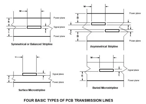
Impedance simulation calculates the characteristic impedance of traces and verifies tolerances across manufacturing variations. Microstrip and stripline configurations require precise stackup definitions, including dielectric thickness and copper weight. As per IPC-2141A guidelines, controlled impedance prevents reflections that degrade signal quality. Field solvers compute Z0 using cross-sectional geometry, accounting for etch factors and surface roughness. Tolerance stacks from material properties and fab processes are analyzed to ensure compliance, typically targeting ±10% or better. This simulation integrates with routing to maintain consistent widths and spacing.
Post-etch simulations incorporate trapezoidal profiles for realism, while temperature and humidity effects on dielectrics are modeled for robustness. Engineers use these results to select laminate Dk and Df values suited to the frequency band. Discontinuities like bends or tees are tuned for minimal impedance perturbation. Impedance simulation thus ensures transmission line integrity throughout the PCB.
Related Reading: PCB Impedance Simulation: Tools and Techniques for Accurate Design
EMI Simulation PCB Analysis
EMI simulation PCB techniques predict radiated and conducted emissions from PCB structures. Power planes and return currents form loop antennas if not segmented properly. Near-field solvers compute coupling between traces and planes, identifying hot spots for shielding. Full-wave 3D simulations capture cavity resonances in multilayer boards, crucial for frequencies above 1 GHz. Engineers optimize guard traces, stitching vias, and ground pours based on these results. EMI simulation PCB reduces the risk of redesigns to meet regulatory limits.
Time-gating in simulations distinguishes far-field radiation from local coupling. Integration with signal integrity tools reveals simultaneous switching noise contributions to EMI. Best results come from hybrid solvers combining 2D/3D methods for efficiency. This comprehensive approach minimizes emissions without over-shielding.
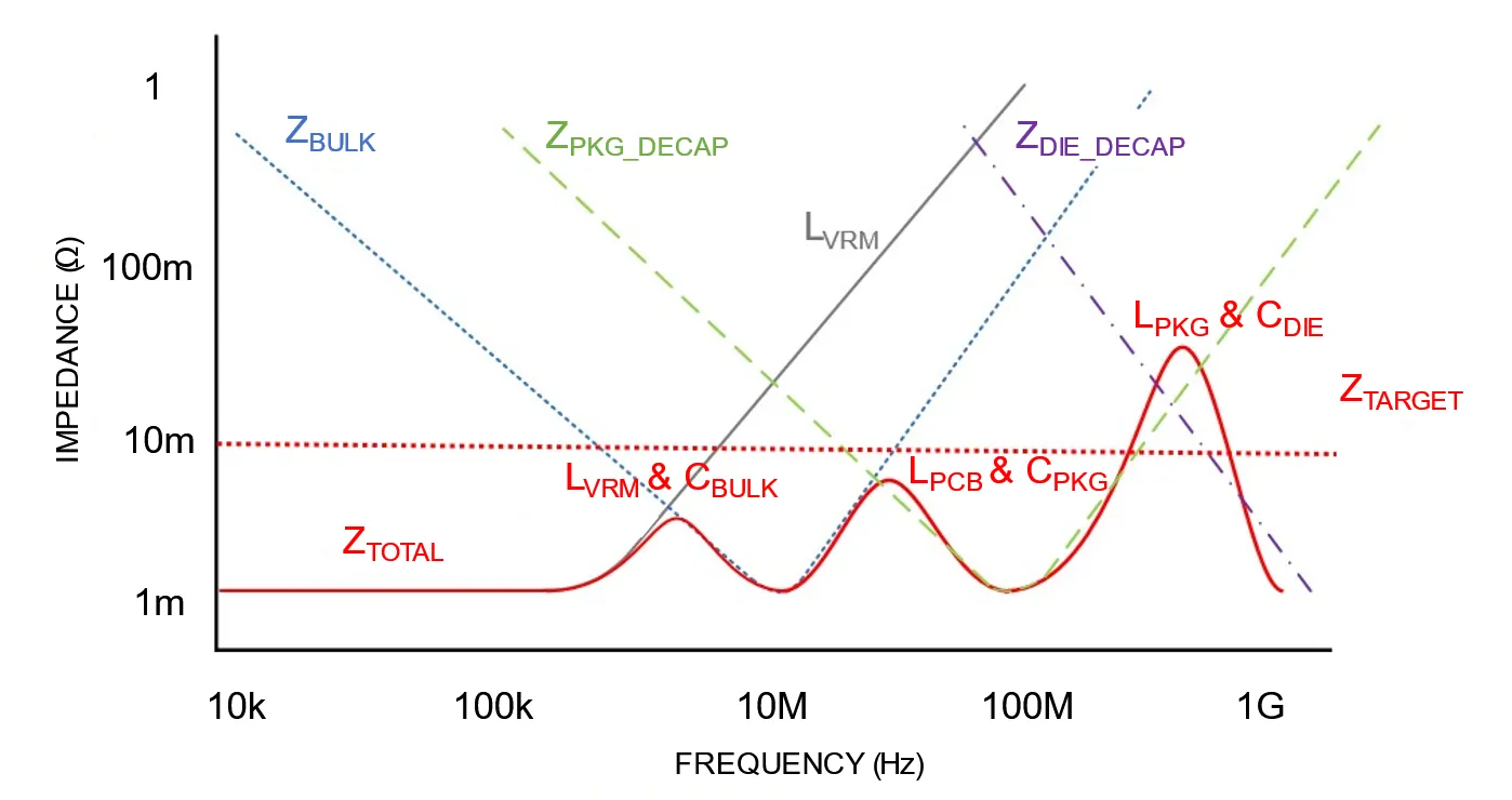
Power Integrity and Its Role
Power integrity simulation complements signal analysis by ensuring stable voltage delivery under dynamic loads. Decoupling capacitor placement is optimized to suppress simultaneous switching noise. PDN impedance targets are set below noise floors across the frequency spectrum. Simulations extract loop inductances and plane resonances, guiding via fencing strategies. Crosstalk between power and signal nets is quantified. Together with other simulations, it forms a holistic high-frequency design verification.
Integrating Simulations into the PCB Design Workflow
The design workflow begins with stackup planning using impedance simulation to define layer thicknesses and materials. Schematic capture incorporates IBIS models for initial signal integrity checks. During placement, EMI pre-scans identify noisy component clusters. Routing employs real-time PCB design software simulation for length matching and impedance control. Post-layout, full 3D extraction feeds hyperlynx-like analyses for S-parameters and eye diagrams. Verification against IPC-6012F performance specs confirms viability before tape-out.
Iteration loops refine the design, with what-if scenarios testing alternatives. Co-simulation with system-level models captures package and connector effects. Documentation of simulation results supports design reviews. This structured integration maximizes the value of high-frequency PCB simulation tools.
Best Practices for Effective Simulation
Start with accurate material models, including frequency-dependent Dk and Df from datasheets. Calibrate simulations against known TDR measurements for validation. Use mesh convergence studies to ensure numerical accuracy in field solvers. Automate post-layout extraction to handle complex geometries. Collaborate across teams by sharing simulation decks. Avoid over-optimization by focusing on dominant effects.
Mesh density increases computation time, so prioritize critical nets. Sensitivity analyses quantify tolerances. Document assumptions and limitations. These practices yield reliable predictions.
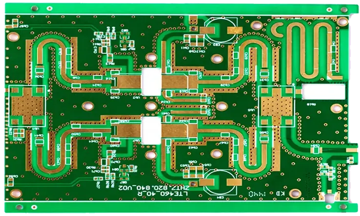
Real-World Application: Troubleshooting a Design Issue
Consider a multilayer board with DDR4 interfaces experiencing eye closure. Initial signal integrity simulation showed via crosstalk exceeding margins. Adjusting via spacing and adding ground vias resolved it. EMI simulation then revealed plane resonance; stitching fixed it. Final impedance checks confirmed 100-ohm differential pairs. Prototyping validated the simulations, avoiding respins.
Such cases highlight simulation's diagnostic power. Engineers learn to trust models through correlation. Iterative refinement builds expertise.
Conclusion
Simulation transforms high-frequency PCB design from trial-and-error to precision engineering. Signal integrity simulation, impedance simulation, and EMI simulation PCB collectively ensure signal fidelity, controlled propagation, and low emissions. PCB design software simulation embeds these capabilities into workflows, aligning with standards like IPC-2141A and IPC-2221C. Engineers adopting these practices achieve first-pass success, reducing costs and time-to-market. As frequencies rise, simulation remains indispensable for innovation and reliability.
FAQs
Q1: What are the primary high-frequency PCB simulation tools used for signal integrity simulation?
A1: High-frequency PCB simulation tools for signal integrity simulation typically include time-domain reflectometry analyzers, IBIS-based transient simulators, and S-parameter extractors. These model reflections, crosstalk, and jitter to predict eye quality. Integration with layout tools enables pre- and post-route verification. Logical setup with accurate models ensures actionable insights for electrical engineers.
Q2: How does impedance simulation improve high-frequency designs?
A2: Impedance simulation computes trace Z0 to prevent mismatches causing reflections, as guided by IPC-2141A. It accounts for stackup variations and guides routing widths. Tolerance analysis ensures fab consistency. This directly enhances signal integrity simulation outcomes in PCB design software simulation.
Q3: Why is EMI simulation PCB critical in multilayer boards?
A3: EMI simulation PCB identifies radiation from plane resonances and trace loops in dense layouts. It optimizes shielding and grounding to minimize emissions. Full-wave analysis captures cavity modes. This prevents compliance failures without hardware testing.
Q4: Can PCB design software simulation replace physical prototypes entirely?
A4: PCB design software simulation significantly reduces prototypes by predicting behaviors accurately. However, validation with measurements is essential due to model assumptions. It excels in iteration speed and cost savings for high-frequency designs.
References
IPC-2141A — Design Guide for High-Speed Controlled Impedance Circuit Boards. IPC, 2004
IPC-2221C — Generic Standard on Printed Board Design. IPC, 2023
IPC-6012F — Qualification and Performance Specification for Rigid Printed Boards. IPC, 2023


