 ALLPCB


Introduction
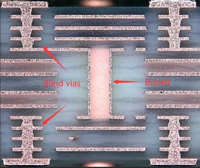
Blind vias represent a critical advancement in modern PCB design, enabling denser interconnects in multilayer boards by connecting surface layers to specific inner layers without penetrating the full stackup. These structures are essential for high-performance electronics where space constraints demand efficient routing. However, blind vias introduce unique challenges, including potential issues with signal integrity, thermal management, and mechanical stress due to their partial-depth drilling and plating processes. Simulation tools play a pivotal role in addressing these concerns through virtual prototyping and performance analysis, allowing engineers to predict and mitigate failures before physical fabrication. By integrating simulation into the PCB design workflow, teams can achieve higher reliability and optimize board performance. This approach aligns with industry demands for robust, compact designs in applications like telecommunications and computing.
Understanding Blind Vias and Their Challenges
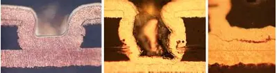
Blind vias differ from through-hole vias by terminating at an inner layer, which reduces stub length and improves signal paths in high-density interconnects. They are typically created using sequential lamination or laser drilling, followed by electroplating to ensure electrical continuity. While blind vias enhance routing density and minimize inductance, they pose manufacturing complexities such as aspect ratio limitations and plating uniformity. Engineers must consider factors like via diameter, landing pad size, and material interactions to prevent defects like cracks or voids. Without proper analysis, these vias can lead to failures under thermal cycling or mechanical shock. Simulation becomes indispensable here, offering a non-destructive method to evaluate these risks early in the PCB design phase.
The relevance of blind vias grows with the push toward finer pitches and more layers in advanced boards. Performance analysis via simulation helps quantify impedance mismatches and crosstalk that through vias might exacerbate. Thermal gradients around blind vias can also cause localized hotspots, affecting component longevity. By modeling these interactions, designers gain insights into real-world behavior, reducing iteration cycles. This proactive strategy ensures compliance with reliability expectations in demanding environments.
Key Technical Principles of Simulation in Blind Via Design
Simulation tools facilitate comprehensive performance analysis by modeling electromagnetic, thermal, and mechanical behaviors specific to blind via structures. In signal integrity simulations, engineers assess via impedance and return loss by solving Maxwell's equations across the via barrel and pads. Blind vias often exhibit lower inductance than through vias due to shorter lengths, but transitions at layer interfaces can introduce discontinuities. Finite element methods discretize the geometry to predict field distributions, revealing potential crosstalk in adjacent vias. Accurate material models, including dielectric constants and copper conductivity, are essential for reliable predictions. These simulations guide trace width adjustments and via staggering to maintain signal quality.
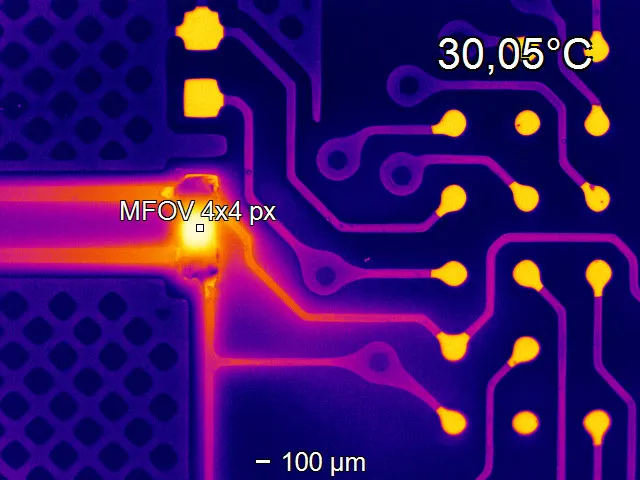
Thermal simulation addresses heat dissipation challenges inherent in blind via configurations. Vias act as thermal conduits, but blind structures limit paths compared to full through vias, potentially creating hotspots under power loads. Finite volume or finite element solvers compute temperature profiles by solving heat transfer equations, incorporating convection, conduction, and radiation boundaries. Engineers can evaluate via fill materials or staggering patterns to enhance spreading. This analysis prevents delamination risks from coefficient of thermal expansion mismatches between copper and substrate. Integrating thermal simulation early optimizes layer stackups for uniform heat flow.
Mechanical simulation evaluates stress concentrations around blind vias, crucial for warpage and fatigue predictions. During lamination or reflow, asymmetric drilling induces residual stresses that simulations capture through linear or nonlinear finite element analysis. Models account for orthotropic material properties of laminates and poisson effects in plating. Blind vias near board edges amplify bending moments, which contour plots visualize effectively. By iterating geometries, engineers minimize crack propagation sites. These insights complement electrical and thermal data for holistic virtual prototyping.
Reliability simulations extend performance analysis to long-term scenarios like thermal cycling. Accelerated models predict via barrel cracking based on strain energy density accumulation. Factors such as plating thickness and via aspect ratio influence fatigue life. Coupled multiphysics simulations link thermal loads to mechanical deformation, offering probabilistic failure rates. This approach aligns with standards like IPC-2221, which provides guidelines for design aspects including via reliability under environmental stresses.
Best Practices for Implementing Simulation in Blind Via PCB Design
Start with accurate geometry import from layout files to ensure simulation fidelity in PCB design workflows. Define boundary conditions realistically, such as power dissipation maps from schematic analysis and ambient temperatures per application. Mesh refinement around via barrels captures steep gradients without excessive computation. Validate models against known benchmarks, like single via test structures, to calibrate solver settings. Iterate designs by adjusting via diameter, pad annular ring, and back-drilling if applicable for stubs.
For signal integrity, perform parametric sweeps on via spacing and stub length to identify optimal configurations. Couple with time-domain reflectometry predictions for eye diagram integrity. In thermal simulation, incorporate anisotropic conductivity of composites and via fill options like conductive epoxy. Monitor junction temperatures against component limits. Mechanical runs should include sequential build-up processes to simulate lamination stresses.
Adopt multiphysics workflows where outputs from one domain feed others, such as thermal results driving mechanical expansion. Document assumptions and sensitivity studies for design reviews. Cross-verify with physical prototypes sparingly, using simulation to de-risk iterations. Standards like IPC-4761 offer guidance on via protection strategies that simulations can evaluate, such as tenting or filling for enhanced robustness. Collaborate across disciplines to integrate simulation insights into manufacturability checks.
Insights from Simulation-Driven Troubleshooting
Engineers often encounter blind via issues like plating voids during high-current operations, detectable via current density simulations revealing hotspots in barrel walls. Adjusting electrolyte models or via geometry mitigates this. Warpage from clustered blind vias appears in mechanical scans as asymmetric deformation; redistributing vias or adding stiffeners resolves it. Signal reflections from mismatched impedances show in S-parameter plots, prompting stub removal or tuning. Thermal runaway in power planes linked to via arrays benefits from redistribution patterns informed by hotspot analysis. These troubleshooting applications underscore simulation's value in rapid root-cause identification.
Conclusion
Simulation tools are indispensable for blind via design, enabling precise performance analysis and virtual prototyping across electrical, thermal, and mechanical domains. By predicting challenges like stress, hotspots, and integrity losses, engineers ensure PCB success without costly respins. Best practices emphasize accurate modeling, multiphysics coupling, and standard-aligned validation. As PCB densities increase, integrating simulation streamlines workflows and boosts reliability. Teams adopting this methodology deliver robust designs ready for production.
FAQs
Q1: What role do simulation tools play in PCB design involving blind vias?
A1: Simulation tools enable virtual prototyping of blind via structures, allowing engineers to analyze signal propagation, thermal distribution, and mechanical stresses before fabrication. They model complex interactions like plating uniformity and layer transitions, optimizing via placement and dimensions. This reduces risks of failures such as crosstalk or delamination, streamlining the design process for high-density boards. Overall, they enhance decision-making with data-driven insights.
Q2: How does thermal simulation contribute to blind via performance analysis?
A2: Thermal simulation maps heat flow through blind vias, identifying hotspots from limited conduction paths compared to through vias. Engineers evaluate stackup effects and fill materials to improve dissipation. It predicts temperature rises under load, preventing reliability issues like electromigration. By iterating virtually, designs achieve balanced thermal management without physical testing delays. This is critical for power-intensive applications.
Q3: Why is virtual prototyping essential for blind via reliability in PCB design?
A3: Virtual prototyping simulates real-world conditions on blind vias, forecasting fatigue from cycling or shock without prototypes. It couples physics domains to reveal coupled effects like thermal-mechanical strain. Engineers refine geometries iteratively, ensuring compliance with reliability thresholds. This method cuts costs and time, delivering verified designs ready for manufacturing. It supports denser interconnects confidently.
Q4: What performance analysis techniques are used with simulation tools for blind vias?
A4: Performance analysis via simulation tools includes impedance profiling, thermal profiling, and stress contouring for blind vias. Time- and frequency-domain solvers assess signal quality, while heat transfer models quantify dissipation. Mechanical finite element analysis predicts warpage risks. These techniques provide quantitative metrics for optimization, ensuring vias meet operational demands across environments.


