ALLPCB


The Role of Pad-to-Pad Spacing in PCB Testing and Troubleshooting
Pad-to-pad spacing plays a critical role in ensuring reliable access during printed circuit board testing and fault diagnosis. Engineers must consider how the distance between test pads influences probe contact, signal integrity, and overall test coverage. In high-density designs, insufficient spacing creates barriers to effective measurement and increases the risk of incomplete fault detection. Proper planning of these distances supports both automated test equipment and manual troubleshooting processes. This consideration becomes especially important as board complexity grows and component miniaturization continues.
What Is Pad-to-Pad Spacing and Why It Matters
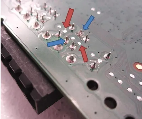
Pad-to-pad spacing refers to the center-to-center or edge-to-edge distance between adjacent test pads or vias designated for probe access. This parameter directly affects the ability of test systems to reach individual nets without mechanical interference or electrical bridging. In practice, adequate spacing enables consistent probe placement, which supports accurate continuity checks, isolation verification, and component value measurements. Insufficient spacing leads to probe placement challenges that reduce test coverage and complicate fault isolation techniques. Industry standards such as IPC-9252 address requirements for electrical testing of unpopulated boards and emphasize the need for accessible test points.
Design teams evaluate spacing early in the layout phase to align with both in-circuit testing and flying probe methods. Larger distances simplify fixture construction for bed-of-nails systems while still allowing flexibility for flying probe equipment. When spacing falls below practical thresholds, engineers face trade-offs between board density and testability. These decisions influence manufacturing yield and long-term reliability because undetected faults can propagate into assembled products. Clear documentation of test point locations and their spacing helps downstream teams maintain consistent quality control.
Technical Principles of Pad Spacing in Testing
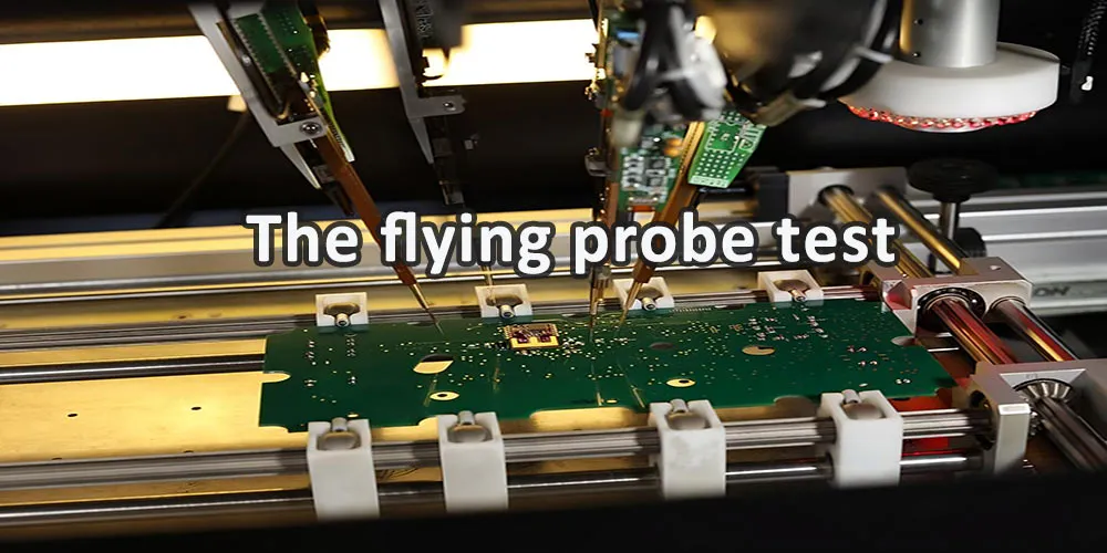
Probe access depends on mechanical tolerances of the test equipment and the physical layout of pads on the board surface. In ICT setups, fixed probes require sufficient clearance to avoid collisions while maintaining reliable electrical contact. Flying probe systems offer more adaptability because movable probes can navigate tighter layouts, yet they still benefit from predictable pad-to-pad distances that reduce positioning errors. The mechanisms involved include probe tip geometry, board flatness, and solder mask registration, all of which interact with spacing to determine contact success rates.
Fault isolation techniques rely on precise measurements between nodes. When pads sit too close together, adjacent signals may experience crosstalk or unintended shorting during probing, which obscures true fault locations. Conversely, generous spacing allows cleaner separation of test signals and supports more thorough adjacency testing as outlined in relevant electrical test specifications. Thermal expansion and mechanical warpage during testing can further alter effective spacing, making initial design margins important for repeatable results.
Engineers also consider via placement and pad size alongside spacing because smaller features demand tighter mechanical control. Standards such as IPC-6012E provide qualification guidance for rigid boards that indirectly supports testability through requirements on pad geometry and plating. Consistent application of these principles across a design reduces variability in test outcomes.
Practical Solutions and Best Practices
Designers achieve reliable PCB test point access by establishing minimum spacing guidelines early and verifying them through design rule checks. Placing test points on a single side of the board simplifies probe access and reduces the need for double-sided fixtures. Distributing points evenly across the layout prevents clustering that could hinder flying probe testing paths or increase fixture complexity. Coordination with test engineering teams ensures that spacing accommodates both current equipment capabilities and future product variants.
Best practices include defining test points for every net that requires verification and maintaining adequate clearance from components and board edges. This approach supports efficient fault isolation techniques by allowing probes to reach critical nodes without obstruction. When high-density constraints arise, selective use of smaller probes or alternative access methods can compensate while preserving overall test coverage. Documentation of spacing decisions aids troubleshooting when boards return from the field or fail during production testing.
Review cycles that incorporate testability feedback help refine spacing before fabrication. Simulation of probe paths and clearance checks further validate the layout against practical equipment limitations. These steps collectively improve first-pass yield and reduce the time required for root-cause analysis during troubleshooting.
Troubleshooting Insights for Engineers
When test failures occur, insufficient pad-to-pad spacing often appears as intermittent contact or missed nodes during ICT or flying probe runs. Engineers troubleshoot by examining probe wear patterns and comparing actual board measurements against design intent. Adjusting fixture pressure or probe selection can sometimes overcome marginal spacing, yet redesign remains the most robust long-term solution. Systematic mapping of failed test points reveals patterns that point back to layout decisions made during initial placement.
Fault isolation becomes more reliable when spacing allows clear differentiation between adjacent nets. In cases where redesign is not feasible, technicians may employ manual probing with finer tips or boundary-scan techniques to supplement automated methods. Consistent application of spacing rules across product families reduces the frequency of such interventions and supports faster diagnosis cycles.
Conclusion
Pad-to-pad spacing forms a foundational element of effective PCB testing strategies. Attention to this parameter improves probe access, supports accurate fault isolation, and aligns designs with established electrical testing practices. Structured consideration during layout yields measurable benefits in manufacturing efficiency and product reliability. Engineers who integrate these principles early achieve more robust test coverage without compromising board density goals.
FAQs
Q1: How does pad-to-pad spacing affect PCB test point access?
A1: Adequate spacing between test pads ensures that probes can reach designated points reliably during both ICT and flying probe testing. Insufficient distances create mechanical interference and reduce the number of accessible nets, which limits overall test coverage and complicates subsequent troubleshooting efforts.
Q2: What spacing considerations apply to ICT testing pad spacing?
A2: ICT testing pad spacing must accommodate fixed probe arrays while providing clearance from components and other features. Designs that follow practical center-to-center distances support stable fixture operation and consistent electrical measurements across production batches.
Q3: How does spacing influence flying probe testing performance?
A3: Flying probe systems benefit from predictable pad-to-pad spacing that allows accurate positioning and minimizes travel time between test locations. Proper distances reduce the risk of probe misalignment and support thorough verification of net connectivity and isolation.
Q4: What role does spacing play in fault isolation techniques?
A4: Clear spacing between test pads enables precise probing of individual nodes, which improves the accuracy of fault localization. This separation reduces signal interference during measurements and helps engineers distinguish between true defects and test artifacts.