 ALLPCB


Introduction
High-density interconnect printed circuit boards continue to shape the trajectory of modern electronics by enabling greater functionality within smaller footprints. Engineers across multiple sectors rely on these boards to meet demands for higher signal speeds, improved thermal performance, and increased component density. As device complexity grows, HDI technology provides the structural foundation that supports next-generation innovations in computing, communications, and sensing systems. The evolution of HDI PCBs reflects ongoing refinements in materials, fabrication processes, and design methodologies that align with established industry practices.
What Are HDI PCBs and Why They Matter
HDI PCBs feature finer conductor lines, smaller vias, and higher layer counts compared with conventional boards, allowing more interconnections per unit area. This architecture supports the integration of advanced components such as microprocessors, memory modules, and radio-frequency circuits without increasing overall board size. Industry relevance stems from the need to accommodate miniaturization trends while maintaining electrical integrity and mechanical reliability. Engineers evaluate HDI designs when conventional routing cannot satisfy performance targets for power delivery or signal integrity. The technology roadmap for HDI emphasizes progressive reductions in feature sizes alongside improvements in via formation and dielectric materials.
Technical Principles of HDI Technology
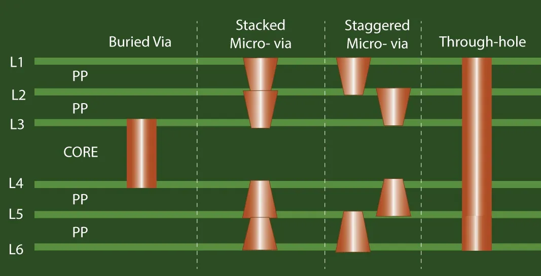
HDI construction relies on sequential lamination processes that incorporate laser-drilled microvias, typically with diameters below 150 micrometers, to connect inner and outer layers efficiently. These microvias reduce the need for through-holes that consume valuable routing space and can introduce parasitic effects at high frequencies. Layer stackups often combine core layers with build-up films that provide controlled impedance environments for differential pairs and high-speed signals. Thermal management considerations include the placement of thermal vias and the selection of dielectric materials with appropriate glass-transition temperatures to withstand reflow cycles. Design rules must account for aspect ratios in vias and the registration tolerances that arise during multiple lamination steps.
Related Reading: HDI PCBs: Benefits, Design Tips, and Manufacturing Techniques
Advancements and Technology Roadmap
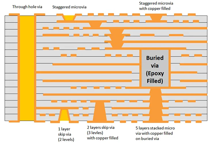
Recent advancements focus on achieving line widths and spaces below 50 micrometers while maintaining yield rates suitable for volume production. New dielectric formulations offer lower dielectric constants and improved dimensional stability, supporting higher-frequency applications up to millimeter-wave bands. The technology roadmap projects continued adoption of any-layer via structures that allow flexible routing across all layers without sequential limitations. Engineers track these developments to anticipate requirements for emerging interfaces such as high-speed serial links and dense sensor arrays. Manufacturing refinements emphasize tighter process controls to meet the acceptance criteria outlined in relevant standards.
Emerging Applications Driving HDI Adoption
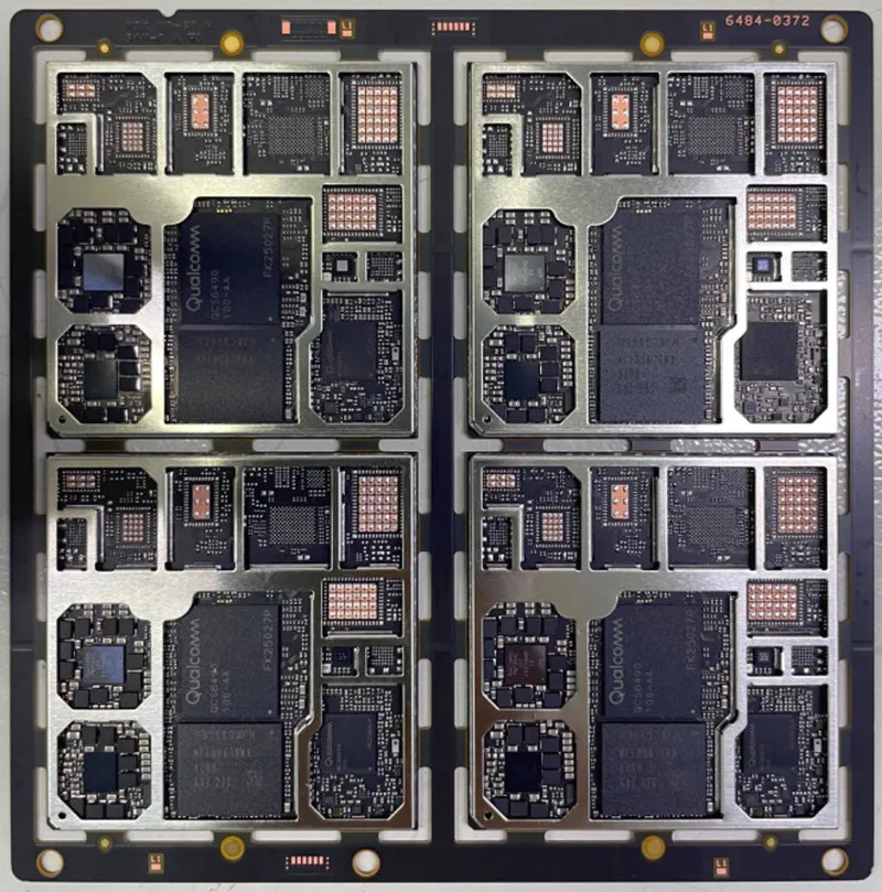
HDI PCBs find increasing use in automotive electronics where space constraints coexist with requirements for vibration resistance and extended temperature operation. In medical devices, the technology enables compact implantable or wearable systems that combine sensing, processing, and wireless communication functions. Telecommunications infrastructure benefits from HDI boards that support massive multiple-input multiple-output antenna arrays and baseband processing units. Industrial automation equipment incorporates HDI designs to integrate power management, control logic, and communication interfaces within rugged enclosures. These applications illustrate how HDI advancements translate into practical system-level improvements without compromising reliability.
Related Reading: HDI PCB Design for High Speed Applications: Overcoming Density Challenges
Best Practices in Design and Manufacturing
Design teams begin with thorough stackup planning that balances electrical performance, thermal dissipation, and manufacturability constraints. Simulation tools help verify signal integrity and power integrity before committing to fabrication, reducing the risk of costly iterations. During manufacturing, adherence to qualification and performance specifications ensures consistent quality across production lots. Engineers specify acceptance criteria for features such as via fill quality and surface finish uniformity to support subsequent assembly steps. Collaboration between design and fabrication teams early in the project helps align expectations with achievable tolerances.
Conclusion
HDI PCBs remain central to the ongoing miniaturization and performance gains observed across electronics platforms. Continued refinements in via technology, materials, and process controls will sustain their role in supporting future device generations. Engineers who incorporate these considerations into their workflows position their designs for compatibility with evolving application requirements. The technology provides a scalable pathway that balances density, reliability, and cost when executed according to established engineering practices.
FAQs
Q1: What defines the future of HDI PCB technology in electronics design?
A1: The future of HDI PCB centers on progressively finer features, advanced via structures, and materials that support higher data rates and greater component integration. Engineers assess these trends when planning systems that require both miniaturization and sustained electrical performance. Industry standards guide the qualification of new constructions to maintain reliability across operating conditions.
Q2: How do HDI PCB trends influence emerging applications in automotive and medical fields?
A2: HDI PCB trends enable compact modules that combine sensing, processing, and communication within space-limited environments typical of automotive control units and medical wearables. These boards accommodate the density needed for advanced driver-assistance systems and diagnostic equipment while meeting thermal and mechanical demands. Practical design choices prioritize via placement and material selection to ensure long-term operation.
Q3: What elements appear on the HDI PCB technology roadmap for the next several years?
A3: The HDI PCB technology roadmap highlights continued reduction in line widths, adoption of any-layer via configurations, and dielectric improvements that lower signal loss at elevated frequencies. Engineers monitor these developments to align board capabilities with interface standards for high-speed serial links and sensor arrays. Manufacturing process controls evolve in parallel to support higher yields at these tighter geometries.
Q4: Which HDI PCB advancements most affect signal integrity in high-speed designs?
A4: HDI PCB advancements such as laser-drilled microvias and low-loss build-up dielectrics reduce discontinuities that degrade signal quality at multi-gigabit rates. Engineers apply controlled-impedance routing and optimized return paths to leverage these improvements. Compliance with relevant performance specifications helps verify that the finished boards meet target electrical parameters.





