 ALLPCB


Creating a compact PCB design with optimized trace spacing is a critical skill for modern electronics engineers. As devices become smaller and more powerful, the demand for high-density interconnect (HDI) layouts and miniaturization continues to grow. But how do you achieve a balance between compactness and functionality while ensuring signal integrity? This blog post dives deep into the art of compact PCB design, focusing on trace spacing optimization, HDI techniques, and effective circuit board layout strategies. Whether you're designing for consumer electronics, medical devices, or automotive systems, you'll find actionable tips to elevate your PCB designs.
Why Compact PCB Design Matters in Today’s Electronics
In the fast-paced world of electronics, smaller is often better. Compact PCB design allows for lighter, more portable devices without sacrificing performance. From smartphones to wearable tech, miniaturization is at the heart of innovation. However, shrinking a circuit board layout comes with challenges like signal interference, heat buildup, and manufacturing constraints. Optimizing trace spacing—the distance between conductive paths on a PCB—is one of the most effective ways to tackle these issues. Proper spacing ensures electrical performance, reduces crosstalk, and meets the strict requirements of HDI designs.
Beyond functionality, compact designs also lower production costs by using less material. With the right approach to trace spacing and layout, you can pack more components into a smaller area while maintaining reliability. Let’s explore the key elements that make this possible.
Understanding Trace Spacing in PCB Design
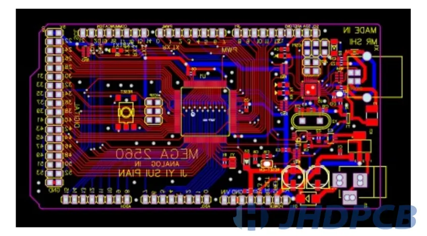
Trace spacing refers to the distance between two adjacent conductive paths (traces) on a PCB. This spacing is crucial for preventing electrical interference, maintaining signal integrity, and ensuring the board can be manufactured without issues. In compact PCB designs, where space is limited, finding the right balance in trace spacing becomes even more important.
In standard designs, trace spacing might range from 6 to 10 mils (0.006 to 0.010 inches) for general-purpose boards. However, in HDI layouts, this can shrink to 3 mils or less. The smaller the spacing, the higher the risk of problems like crosstalk—where signals from one trace interfere with another—or short circuits during manufacturing. To avoid these, designers must adhere to specific guidelines based on the board’s purpose and the manufacturer’s capabilities.
Trace spacing also depends on the voltage levels involved. For high-voltage applications, wider spacing (often 20 mils or more) is needed to prevent arcing. For low-voltage digital circuits, tighter spacing can work, but signal speed and impedance must be considered. For example, a high-speed signal at 5 GHz may require controlled impedance of 50 ohms, which directly affects trace width and spacing.
The Role of HDI in Miniaturization
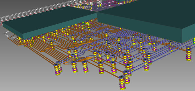
High-Density Interconnect (HDI) technology is a game-changer for compact PCB design. HDI boards use microvias, blind vias, and buried vias to create denser connections in smaller spaces. This allows for more layers and components in a reduced footprint, making HDI ideal for applications like 5G devices, medical implants, and automotive sensors.
In HDI designs, trace spacing often drops below 4 mils, and line widths can be as narrow as 2 mils. These ultra-fine features enable miniaturization but demand precision in layout and manufacturing. Microvias, for instance, with diameters as small as 0.004 inches, connect layers without taking up much surface area. However, such tight spacing increases the risk of signal integrity issues, so careful planning is essential.

Key Strategies for Optimizing Trace Spacing in Compact Designs
Achieving optimized trace spacing in compact PCB design requires a mix of technical know-how and practical strategies. Below are some proven approaches to help you create efficient, reliable layouts.
1. Prioritize Signal Integrity with Controlled Impedance
High-speed signals, common in compact designs, are sensitive to trace spacing and width. To maintain signal integrity, you need controlled impedance, which ensures that the trace dimensions match the required resistance (often 50 or 75 ohms for RF applications). Use PCB design software to calculate the ideal spacing and width based on your board’s dielectric material and layer stack-up. For instance, a 50-ohm impedance trace on a standard FR-4 material might need a width of 6 mils and spacing of 5 mils on a 0.062-inch thick board.
2. Minimize Crosstalk with Proper Spacing
Crosstalk happens when traces are too close, causing electromagnetic interference between signals. To reduce this, increase spacing between high-speed traces or use ground planes to shield them. A general rule is to keep spacing at least three times the trace width for critical signals. For example, if your trace is 5 mils wide, aim for a spacing of 15 mils where possible. In HDI layouts with limited room, consider routing sensitive traces on different layers.
3. Follow Design for Manufacturing (DFM) Guidelines
Manufacturing limitations often dictate trace spacing in compact designs. Most manufacturers have minimum spacing rules, typically 3 to 5 mils for HDI boards. Exceeding these limits risks defects like short circuits during etching. Always check with your fabrication partner to confirm their capabilities before finalizing your circuit board layout. This step prevents costly redesigns and ensures your compact PCB can be produced reliably.
4. Use Layer Stacking to Your Advantage
In HDI designs, stacking multiple layers allows you to route traces in a smaller surface area. Alternate signal and ground layers to reduce interference and maintain tight spacing. For instance, a 6-layer HDI board might have signal traces on layers 1, 3, and 5, with ground planes on layers 2, 4, and 6. This setup not only saves space but also improves electrical performance by providing a return path for signals.
5. Leverage Advanced Tools for Precision
Modern PCB design software offers features like auto-routing and design rule checks (DRC) to optimize trace spacing. These tools can flag spacing violations and suggest adjustments, saving time in complex HDI layouts. Some platforms even simulate signal behavior to predict issues like crosstalk before manufacturing. Investing in such tools is crucial for achieving precision in compact designs.
Common Challenges in Compact PCB Design and How to Overcome Them
While compact PCB design offers many benefits, it also presents unique challenges. Here’s how to address some of the most common issues related to trace spacing and miniaturization.
Thermal Management in Tight Spaces
Dense layouts generate more heat, which can affect performance and reliability. To manage this, ensure adequate spacing around high-power components and use thermal vias to dissipate heat to other layers. For example, placing thermal vias with a diameter of 0.012 inches under a power IC can reduce hotspot temperatures by up to 20°C.
Signal Integrity at High Speeds
As trace spacing decreases, the risk of signal degradation increases, especially for high-speed data like USB 3.0 or PCIe. Use differential pair routing for critical signals, maintaining equal trace lengths and consistent spacing (often 5 mils) to avoid timing issues. Adding ground vias near signal transitions can also stabilize performance.
Manufacturing Constraints
Not all manufacturers can handle ultra-fine trace spacing or HDI features like microvias. Partner with a fabrication house experienced in compact designs to avoid production delays. Request a detailed capability sheet to understand their minimum spacing (e.g., 3 mils) and via size limits before starting your layout.
Practical Tips for Effective Circuit Board Layout in Miniaturization
Beyond trace spacing, a well-thought-out circuit board layout is essential for successful miniaturization. Here are some tips to streamline your design process.
- Group Components Logically: Place related components close together to shorten trace lengths and reduce spacing needs. For example, keep a microcontroller near its supporting capacitors and resistors to minimize signal delays.
- Optimize Via Placement: In HDI designs, use vias-in-pad to save space, but ensure your manufacturer supports this technique. Blind and buried vias can also free up surface area for tighter layouts.
- Plan for Testing and Assembly: Even in compact designs, leave room for test points and assembly clearances. A spacing of 50 mils around test pads ensures accessibility without compromising density.
Future Trends in Compact PCB Design and Trace Spacing
The field of PCB design is evolving rapidly, with new technologies shaping the future of miniaturization. Flexible and rigid-flex PCBs are gaining traction for wearable and foldable devices, requiring even tighter trace spacing. Additionally, advancements in materials, like low-loss dielectrics, are enabling finer traces for high-frequency applications above 10 GHz.
Artificial intelligence (AI) is also making its way into design tools, automating trace spacing optimization and predicting signal issues before they occur. As these technologies mature, engineers will have more resources to push the boundaries of compact PCB design.
Conclusion: Mastering the Art of Compact PCB Design
Compact PCB design is both an art and a science, requiring a deep understanding of trace spacing, HDI techniques, and circuit board layout. By optimizing trace spacing, you can achieve miniaturization without sacrificing signal integrity or manufacturability. From controlling impedance to managing thermal challenges, every detail counts in creating a reliable, high-performance design.
Whether you’re working on a cutting-edge 5G device or a simple IoT sensor, the strategies outlined in this guide can help you navigate the complexities of compact layouts. Focus on precision, collaborate with your manufacturing partner, and leverage modern tools to bring your vision to life. With the right approach, you’ll master the art of compact PCB design and stay ahead in the ever-shrinking world of electronics.


