 ALLPCB


Introduction
Stencil printing and pin-in-paste (PIP) technology represent a key advancement in mixed-technology PCB assembly, allowing through-hole components to be soldered alongside surface-mount devices during a single reflow process. This approach eliminates the need for separate wave soldering or hand soldering steps, streamlining production and reducing costs for low-to-medium volume runs. Electrical engineers often encounter challenges in achieving reliable solder joints with PIP due to variations in paste deposition and reflow dynamics. Understanding stencil printing specifics for PIP ensures consistent solder paste volume for through-hole vias, minimizing defects like insufficient fill or bridging. This guide explores the principles, design considerations, and troubleshooting strategies to optimize stencil printing pin in paste processes.
What Is Stencil Printing and Pin-in-Paste Technology?
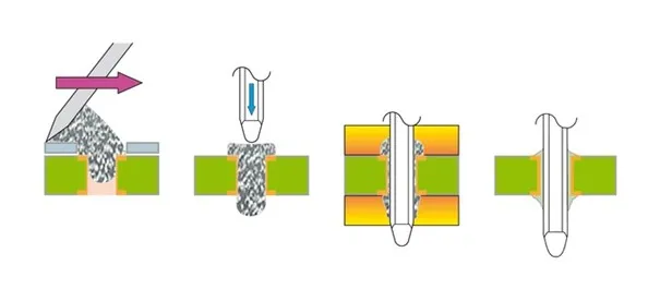
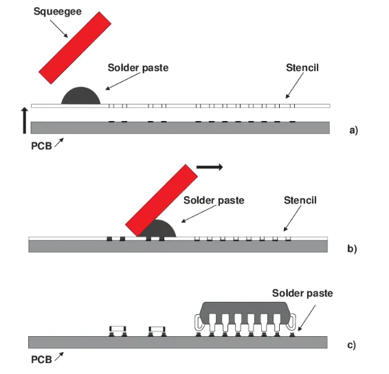
Stencil printing involves applying solder paste through a metal stencil onto PCB pads and vias using a squeegee blade, creating precise deposits for component attachment. In pin-in-paste technology, this process extends to through-hole components by forcing paste into plated through-holes, which pins then displace during placement. After placement, the assembly enters reflow soldering, where the paste melts to form fillets around the pins and secure connections. This method suits prototypes or boards with few through-hole parts, avoiding dedicated wave solder lines. Engineers value PIP for its compatibility with standard SMT equipment, though it demands careful control over paste rheology and stencil geometry to prevent voids or slumping.
The relevance of stencil printing pin in paste grows in high-mix, low-volume environments where flexibility trumps high-speed throughput. Traditional through-hole soldering relies on wave or selective processes, but PIP integrates seamlessly into SMT lines, cutting handling risks and thermal stress variations. However, success hinges on delivering adequate solder paste volume for through hole components to wet barrel walls and form proper fillets. Poor execution leads to common issues like open joints or pin floating, underscoring the need for process validation.
Technical Principles of Stencil Printing in PIP
During stencil printing for PIP, the squeegee pressure and speed push solder paste into through-holes, relying on the paste's thixotropy to hold shape without excessive flow-out. Aperture design plays a critical role, as undersized openings restrict fill while oversized ones cause bridging to adjacent pads. Paste transfer efficiency depends on stencil thickness, typically balanced against fine-pitch SMT needs, but PIP often requires adjustments to prioritize via filling. Separation speed from the board must be controlled to avoid paste smear or pull-back, ensuring clean deposits. Reflow then relies on the deposited volume to alloy properly around the inserted pin.
Paste composition affects PIP performance, with high tackiness preventing premature slump from hole bottoms and metal loading influencing melt flow. Inadequate volume leaves air pockets or unwetted barrels, while excess can lead to blowholes from flux volatiles. Engineers troubleshoot by inspecting paste height post-print using SPI (solder paste inspection) tools, correlating volume to hole geometry. IPC-7525 provides guidelines for stencil fabrication and aperture rules applicable to PIP printing challenges.
Related Reading: Understanding Stencil Printing: A Comprehensive Guide for SMT Assembly
Stencil Design for PIP
Stencil design for PIP demands apertures larger than the through-hole diameter to deposit sufficient paste, often approaching 110-130% of hole size based on process trials. Rounded or trapezoidal apertures improve paste release and reduce bridging risks compared to sharp squares. For mixed boards, multi-level or stepped stencils allow thicker deposits over through-holes without compromising SMT pad volumes. Laser-cut stencils with electropolished surfaces enhance paste release, minimizing residue and ensuring consistent transfer ratios above 75%. Fiducials and alignment marks must align precisely to sub-micron levels for high-density boards.
Aperture walls should feature optimal polish to balance release and shear, avoiding dog-boning where paste volume concentrates at ends. In PIP, overprinting onto solder mask around holes adds fillet material post-insertion. Engineers iterate designs using simulation software to predict volumes before fabrication. J-STD-001 outlines requirements for intrusive soldering processes like paste-in-hole, emphasizing hole fill criteria.
- Aperture Size — Larger than hole diameter: Ensures paste fill
- Shape — Rounded/trapezoidal: Improves release
- Thickness — Stepped or thicker over TH: Balances SMT/TH needs
- Surface Finish — Electropolished: Consistent transfer
- Multi-Level — Yes for mixed tech: Volume control
Related Reading: Solder Paste Stencil Design: Key Factors for Perfect PCB Printing
Solder Paste Volume for Through-Hole Components
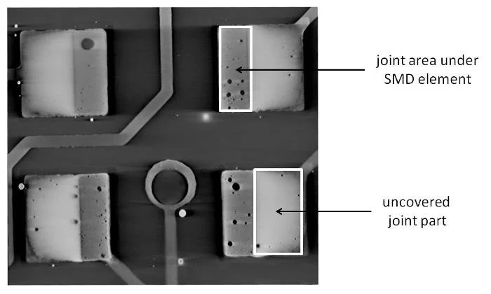
Determining solder paste volume for through hole in PIP starts with calculating the via barrel volume minus pin displacement, plus required fillet heights on both sides. Formulas account for plated barrel thickness, hole aspect ratio, and desired heel/toe fillet dimensions per class of assembly. Too little paste results in barrel voids detectable via X-ray, while excess promotes solder balls or bridging during reflow. Paste metal content around 85-90% aids wetting, but viscosity must hold vertical fill against gravity.
Process controls like print pressure (typically 1-5 kg) and snap-off distance optimize deposition. Validation involves sectioning samples or 3D SPI to measure effective volume post-print. Troubleshooting low fill often traces to stencil misalignment or worn squeegees, addressed by routine maintenance. IPC-610 acceptability criteria guide post-reflow joint evaluation, focusing on fill percentage and fillet formation.
Best Practices and Troubleshooting for Stencil Printing Pin in Paste
Select solder paste with strong tack for PIP to retain paste under pins during placement vibrations. Implement two-stage printing for high-volume holes: first fill vias deeply, then top with SMT paste using a secondary stencil. Reflow profiles should include extended pre-soak for flux activation and peak temps matching paste specs to avoid hot slump. Clean stencils between prints with approved wipes to prevent bridging from dried residue.
Common defects include insufficient hole fill from low pressure, fixed by increasing squeegee force incrementally. Pin float occurs if paste slumps; counter with higher viscosity pastes or board preheat. Bridging between vias and pads demands aperture spacing reviews per IPC-7525 rules. SPI integration catches 80% of print issues pre-placement, enabling real-time adjustments.
For troubleshooting:
- Voids in barrel: Increase aperture size or print passes.
- Paste smear: Reduce separation speed.
- Inconsistent volume: Calibrate printer pressure uniformly.
- Fillet shortfall: Add mask overprint or adjust reflow soak.
Validate processes with cross-sections per J-STD-001 to confirm 100% barrel fill for Class 3 assemblies.
Conclusion
Stencil printing pin in paste technology offers electrical engineers a versatile solution for mixed SMT/through-hole boards, optimizing assembly efficiency when executed with precision. Key to success lies in tailored stencil design for PIP, accurate solder paste volume for through hole components, and rigorous process controls. By adhering to standards like IPC-7525 and J-STD-001, teams achieve reliable joints without secondary soldering. Troubleshooting empowers quick iterations, ensuring high yields even in complex designs. Mastering these elements positions PIP as a go-to for modern PCB fabrication challenges.
FAQs
Q1: What is the role of stencil design for PIP in achieving proper solder paste volume for through hole components?
A1: Stencil design for PIP enlarges apertures over through-holes to deposit adequate paste, compensating for pin displacement and fillet needs. Stepped stencils balance this with SMT requirements, preventing underfill. Practical tip: Simulate volumes pre-print to validate against J-STD-001 criteria, reducing voids via iterative adjustments. This ensures reflow forms compliant joints without excess bridging.
Q2: How does stencil printing pin in paste differ from standard SMT printing?
A2: Stencil printing pin in paste forces paste into vias for through-hole soldering during reflow, unlike SMT's pad-only focus. It requires larger, shaped apertures and tackier paste to hold vertical deposits. Troubleshooting involves SPI for volume checks and pressure tweaks to avoid slump. This integration cuts processes but demands precise alignment for mixed boards.
Q3: What are common troubleshooting steps for insufficient solder paste volume for through hole in PIP?
A3: Inspect stencil apertures for size and polish, then adjust print pressure upward. Verify paste tackiness and use two-stage printing for deep fills. Post-print SPI measures volume against hole geometry. Reflow tweaks like longer soak address residual issues. Cross-section analysis confirms fixes per IPC-610 standards.
Q4: Why reference IPC-7525 for stencil printing pin in paste processes?
A4: IPC-7525 guides aperture design and fabrication for reliable paste transfer in PIP, covering ratios and finishes. It helps engineers optimize for through-hole fill without SMT compromise. Apply rules to avoid defects like bridging, ensuring consistent volumes. This standard streamlines validation for production scalability.
References
IPC-7525C — Stencil Design Guidelines. IPC, 2021
J-STD-001G — Requirements for Soldered Electrical and Electronic Assemblies. IPC, 2017
IPC-610H — Acceptability of Electronic Assemblies. IPC, 2019


