 ALLPCB


In the world of printed circuit board (PCB) design, achieving optimal signal integrity is crucial, especially for high-speed and high-frequency applications. One of the key factors in ensuring this is PCB signal layer impedance control. But what exactly is signal layer impedance, and how can you control it to maintain signal quality? In short, signal layer impedance control involves designing traces and layers on a PCB to have a specific resistance to signal flow, preventing issues like reflections and crosstalk that degrade performance. This blog dives deep into the essentials of impedance matching, controlled impedance traces, the differences between microstrip vs. stripline, and methods for signal layer impedance calculation. Let’s explore how to master these concepts for better PCB designs.
What Is Signal Layer Impedance and Why Does It Matter?
Signal layer impedance refers to the resistance a signal encounters as it travels along a trace on a specific layer of a PCB. In high-speed circuits, if this impedance isn’t properly managed, signals can reflect back, causing data errors, noise, or even complete signal failure. This is especially critical in applications like telecommunications, automotive electronics, and computing, where signals operate at gigahertz frequencies.
Proper impedance control ensures that signals travel smoothly from source to destination without distortion. It minimizes issues like crosstalk (interference between adjacent traces) and electromagnetic interference (EMI). By maintaining consistent impedance, you can achieve reliable performance, reduce design iterations, and save costs in the long run.
Understanding Impedance Matching in PCB Design
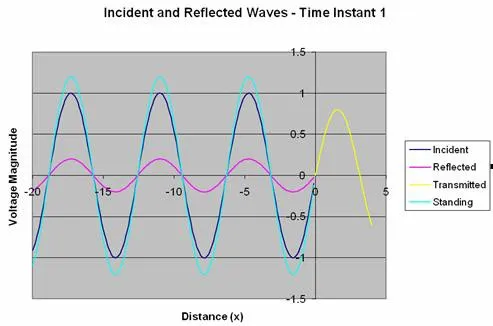
Impedance matching is the process of designing a PCB so that the impedance of the source, transmission line (trace), and load are equal. When these are mismatched, a portion of the signal reflects back toward the source, leading to signal loss and potential errors. For instance, in a high-speed USB design, a common target impedance is 90 ohms for differential pairs. If the trace impedance deviates from this value, data transmission can become unreliable.
To achieve impedance matching, designers adjust trace width, spacing, and the dielectric material between layers. Tools like impedance calculators and simulation software help predict and fine-tune these parameters during the design phase. The goal is to ensure that signals arrive at their destination with minimal distortion, maintaining the integrity of the data being transmitted.
Key Benefits of Impedance Matching
- Reduces signal reflections and ensures clean transmission.
- Improves power transfer efficiency between components.
- Minimizes noise and EMI in high-frequency circuits.
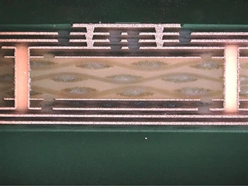
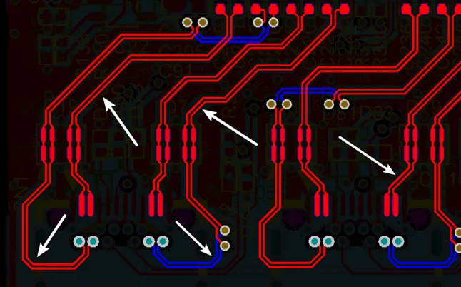
Controlled Impedance Traces: The Backbone of Signal Integrity
Controlled impedance traces are traces on a PCB designed to have a specific impedance value, often determined by the requirements of the circuit. For example, a typical single-ended trace might target 50 ohms, a standard for many RF applications. Controlling impedance involves precise calculations and manufacturing techniques to maintain consistency across the board.
Factors that influence trace impedance include:
- Trace Width: Wider traces have lower impedance, while narrower traces have higher impedance.
- Trace Thickness: Thicker copper reduces impedance slightly.
- Dielectric Constant: The material between layers affects how signals propagate. A lower dielectric constant (e.g., 3.2 for some high-speed materials) results in higher impedance.
- Layer Spacing: The distance between a trace and its reference plane (ground or power) impacts impedance.
During manufacturing, maintaining tight tolerances is essential. Even a small deviation in trace width or dielectric thickness can alter impedance, affecting performance. Designers often collaborate closely with fabricators to ensure these parameters are met.
Microstrip vs. Stripline: Choosing the Right Configuration
When designing for impedance control, one key decision is whether to use a microstrip or a stripline configuration for your traces. Both have unique characteristics that impact signal integrity, impedance, and manufacturing complexity.
What Is a Microstrip?
A microstrip is a trace on the outer layer of a PCB, with a ground plane directly beneath it, separated by a dielectric material. It’s easier to fabricate and inspect since it’s on the surface, but it’s more susceptible to external interference and EMI. Microstrips are often used in simpler designs or where cost is a concern. Their typical impedance range is 50-75 ohms for many applications.
What Is a Stripline?
A stripline, on the other hand, is a trace embedded between two ground planes within the PCB. This configuration offers better shielding from EMI and crosstalk, making it ideal for high-frequency designs. However, striplines are harder to fabricate and test since they’re internal. They often have a slightly lower impedance range compared to microstrips due to the dual reference planes.
Key Differences and When to Use Each
- EMI Protection: Stripline wins with better shielding due to dual ground planes.
- Ease of Fabrication: Microstrip is simpler and cheaper to produce.
- Signal Integrity: Stripline provides superior performance in noisy environments or at very high frequencies (e.g., above 1 GHz).
- Board Space: Microstrip uses outer layers, freeing up internal layers for other signals.
Choosing between microstrip and stripline depends on your project’s requirements. For a 5G communication board, a stripline might be necessary to handle high frequencies with minimal interference. For a low-cost consumer device, a microstrip could suffice.

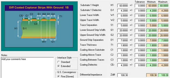
Signal Layer Impedance Calculation: How to Get It Right
Accurate signal layer impedance calculation is the foundation of controlled impedance design. Calculating impedance ensures that traces meet the target value required for your circuit, whether it’s 50 ohms for a single-ended RF line or 100 ohms for a differential pair in high-speed digital designs.
Factors in Impedance Calculation
Impedance depends on several physical and material properties:
- Trace Width (W): Measured in mils or millimeters, wider traces reduce impedance.
- Trace Height (H): The distance from the trace to the reference plane; larger heights increase impedance.
- Dielectric Constant (Er): A property of the PCB material, typically between 3.5 and 4.5 for standard FR-4 materials.
- Trace Thickness (T): Thicker traces slightly lower impedance.
Basic Formula for Microstrip Impedance
For a microstrip, a simplified formula to estimate characteristic impedance (Z0) is:
Z0 = (87 / √(Er + 1.41)) * ln(5.98H / (0.8W + T))
Where:
- Z0 is the characteristic impedance in ohms.
- Er is the dielectric constant.
- H is the height of the dielectric.
- W is the trace width.
- T is the trace thickness.
For a practical example, consider a microstrip on an FR-4 board with Er = 4.2, H = 8 mils, W = 10 mils, and T = 1.4 mils. Plugging these into the formula gives an approximate impedance of 50 ohms, a common target for RF signals.
Tools for Impedance Calculation
While manual calculations provide insight, most designers use software tools or online calculators for precision. These tools account for complex factors like frequency-dependent effects and layer stack-up variations. During the design phase, simulations can validate the calculated impedance before manufacturing begins.
Practical Tips for Achieving Optimal Signal Integrity
Beyond calculations and configurations, several best practices can help maintain signal integrity through impedance control:
- Consistent Layer Stack-Up: Design your PCB stack-up early and stick to it. Changes in layer spacing or materials can alter impedance unexpectedly.
- Minimize Vias: Vias introduce impedance discontinuities. If unavoidable, use back-drilling for high-speed designs to reduce stub effects.
- Reference Planes: Ensure continuous ground or power planes beneath signal traces to provide a stable return path.
- Routing Guidelines: Avoid sharp bends in traces; use 45-degree angles or curves to prevent signal reflections.
- Material Selection: Choose PCB materials with stable dielectric constants for high-frequency applications. For instance, materials with Er values around 3.0-3.5 are often preferred for speeds above 5 GHz.
Implementing these strategies during the design phase can prevent costly rework and ensure your board performs as intended.
Challenges in Signal Layer Impedance Control
Despite best efforts, challenges can arise in achieving perfect impedance control:
- Manufacturing Variations: Small deviations in trace etching or dielectric thickness during fabrication can affect impedance. Tight tolerances (e.g., ±10% for trace width) are often necessary.
- Frequency Dependence: At very high frequencies, skin effect and dielectric losses alter effective impedance, requiring advanced materials or design adjustments.
- Complex Designs: Boards with mixed-signal or high-density layouts may have conflicting impedance requirements, complicating the design process.
Collaboration with your PCB manufacturer is key to overcoming these hurdles. Providing detailed stack-up information and impedance targets ensures the final product matches your design intent.
Conclusion: Mastering Signal Integrity with Impedance Control
Signal layer impedance control is a cornerstone of modern PCB design, ensuring that high-speed and high-frequency signals travel without distortion or interference. By focusing on PCB signal layer impedance, implementing impedance matching, designing controlled impedance traces, choosing between microstrip vs. stripline, and performing accurate signal layer impedance calculation, you can achieve optimal signal integrity for any application.
Whether you’re working on a cutting-edge telecommunications device or a simple consumer product, these principles apply universally. With careful planning, precise calculations, and collaboration with manufacturing partners, you can build reliable, high-performing PCBs that meet the demands of today’s technology. Start integrating these impedance control techniques into your next design, and watch your signal quality soar.


