 ALLPCB


Introduction
Relay contact bounce represents a common challenge in electromechanical relay applications, particularly within PCB designs where precise switching is essential. Electrical engineers often encounter this phenomenon during system integration, leading to unreliable signal processing and premature component wear. Understanding relay contact bounce allows for proactive design strategies that enhance circuit stability and longevity. This article explores the mechanics behind relay bounce, its implications in real-world scenarios, and proven mitigation techniques tailored for PCB assemblies. By addressing relay chattering and implementing relay contact stabilization methods, engineers can achieve robust performance. Key focus areas include debounce circuits and relay bounce mitigation approaches grounded in practical engineering principles.
What Is Relay Contact Bounce and Why It Matters
Relay contact bounce occurs when the mechanical contacts of a relay physically rebound upon closing or opening, resulting in multiple rapid interruptions before achieving a stable state. This bouncing typically manifests as a series of make-break cycles lasting from the initial impact until the contacts settle. In contrast, relay chattering refers to prolonged or excessive bouncing often triggered by external factors like vibration or unstable coil voltage. For electrical engineers working on PCB-based systems, relay contact bounce matters because it introduces noise in digital interfaces, causes erroneous counts in counters or encoders, and generates electromagnetic interference. In power switching applications, it accelerates contact erosion through arcing during each bounce event. Ignoring this issue can lead to system failures, increased maintenance, and non-compliance with reliability expectations in demanding environments.
Technical Principles Behind Relay Contact Bounce
The root cause of relay contact bounce lies in the electromechanical dynamics of the relay armature and contacts. When the coil energizes, the magnetic force pulls the armature toward the stationary contacts with significant momentum. Upon impact, the elastic deformation of contact materials and springs causes rebound, similar to a ball bouncing on a surface. Factors influencing bounce duration include armature mass, spring stiffness, contact gap, and surface finish of the contact points. Higher coil voltages can reduce bounce by increasing impact speed, but excessive force may worsen wear. Contact materials like silver alloys are selected for durability, yet they still exhibit inherent bounce due to these physical properties.
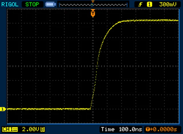
Environmental conditions exacerbate relay contact bounce. Vibration from nearby motors or PCB flexing during operation induces relay chattering, where contacts repeatedly separate under marginal force. Temperature variations alter material elasticity, potentially lengthening bounce times. In PCB assemblies, improper soldering per J-STD-001 standards can introduce mechanical stress, amplifying bounce through pin misalignment or solder joint fatigue. Engineers must consider these interactions during component selection and layout to minimize inherent bounce. Oscilloscope measurements reveal bounce patterns unique to each relay type, guiding targeted mitigation.
Impacts of Relay Contact Bounce in PCB Applications
Unmitigated relay contact bounce disrupts digital logic by registering multiple transitions as separate events. For instance, a single relay closure might trigger several interrupts in a microcontroller, leading to incorrect state machines or data logging errors. In automotive or industrial controls, this translates to false alarms or unsafe operations. Arcing during bounces generates heat and metal transfer, reducing contact life over cycles. Electromagnetic emissions from arcs couple into nearby traces, violating signal integrity on high-speed PCBs. Relay chattering compounds these issues, often signaling deeper problems like power supply ripple.
From a reliability standpoint, persistent bounce accelerates failure modes in high-cycle applications. Contact welding or pitting emerges faster under repeated arcing, necessitating frequent replacements. In densely populated PCBs, bounce-induced noise propagates through ground planes, affecting analog sensors. Compliance with assembly standards like IPC-A-610 ensures visual acceptability but does not directly address bounce; functional testing remains crucial. Engineers prioritizing relay contact stabilization extend system mean time between failures, optimizing total cost of ownership.

Practical Solutions for Relay Bounce Mitigation
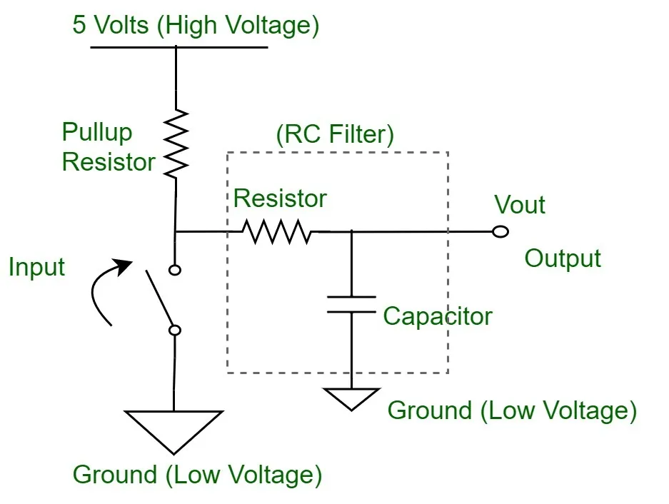
Effective relay bounce mitigation begins with relay selection favoring low-bounce designs, such as those with damped armatures or precious metal contacts. However, supplemental circuits provide reliable relay contact stabilization across variants. A simple debounce circuit uses an RC low-pass filter followed by a Schmitt trigger inverter, filtering transients while preserving edge sharpness. The resistor limits current, and the capacitor charges slowly, suppressing bounces below a threshold. Values around 10kΩ resistor and 100nF capacitor suit many DC signals, adjustable based on bounce duration observed via oscilloscope.
For robust applications, digital debounce circuits employ D-type flip-flops or monostable multivibrators to generate a clean pulse. A 74HC74 flip-flop configuration clocks the relay signal, latching the stable state after bounce settles. This hardware approach excels in noisy environments, independent of software overhead. In power relays handling inductive loads, RC snubber networks across contacts quench arcs, reducing bounce-related erosion. Diode suppression on coil drivers prevents back-EMF, indirectly stabilizing operation. PCB layout supports these by placing debounce components near relay pins, minimizing trace inductance per J-STD-001 guidelines.
Software debounce complements hardware in microcontroller-driven systems. Algorithms sample the relay input multiple times over 10-20 ms, confirming stability before action. Hysteresis in code prevents marginal triggers, ideal for low-frequency switching. Combining methods yields optimal relay bounce mitigation. Vibration isolation via mounting pads curbs relay chattering. Testing post-assembly verifies effectiveness, ensuring clean waveforms.
Troubleshooting Relay Chattering and Advanced Insights
Relay chattering often stems from insufficient coil voltage margin or mechanical shock. Measure coil supply under load; dips below 80% nominal exacerbate issues. External vibration sources require decoupling capacitors on power rails and conformal coating for PCB damping. Inspect solder joints against IPC-A-610 criteria; cracked fillets induce flexing that mimics chatter. Use high-speed scopes to differentiate true bounce from chatter by duration and repeatability.
In high-reliability designs, accelerated life testing simulates bounce cycles. Standards like IEC 61810 for electromechanical relays guide performance specs, emphasizing contact reliability. Firmware counters track bounce events for predictive maintenance. Hybrid solid-state relays eliminate bounce entirely but lack galvanic isolation of mechanical types. Troubleshooting flowcharts streamline diagnosis: scope signal, check voltage, isolate vibration, iterate debounce.
Conclusion
Relay contact bounce remains an inherent challenge in electromechanical switching, but targeted strategies ensure reliable PCB performance. Distinguishing bounce from chattering enables precise diagnosis and intervention. Debounce circuits, optimized layouts, and adherence to standards like J-STD-001 and IEC 61810 deliver relay contact stabilization without complexity. Electrical engineers benefit from integrating hardware, software, and mechanical fixes for comprehensive relay bounce mitigation. Proactive measures extend relay life, reduce EMI, and safeguard system integrity. Implementing these techniques positions designs for enduring success in demanding applications.
FAQs
Q1: What causes relay contact bounce in PCB assemblies?
A1: Relay contact bounce arises from mechanical rebound when the armature strikes contacts, influenced by spring tension, mass, and material elasticity. In PCBs, soldering defects or vibration amplify it, leading to relay chattering. Observing waveforms helps quantify duration, typically resolving in milliseconds. Proper assembly per J-STD-001 minimizes contributions from joint stress. Addressing root causes prevents downstream issues like false triggering.
Q2: How does a debounce circuit mitigate relay bounce?
A2: A debounce circuit filters rapid transients from relay contact bounce using RC networks or logic gates, producing a stable output signal. For example, a Schmitt trigger cleans the filtered edge, ideal for digital inputs. Placement near the relay on the PCB reduces noise pickup. This relay bounce mitigation ensures single-event registration, crucial for counters or PLCs. Tune components based on scoped bounce time for optimal response.
Q3: What differentiates relay chattering from normal contact bounce?
A3: Normal relay contact bounce is brief, self-limiting mechanical oscillation on switching, while relay chattering involves sustained interruptions from vibration, voltage instability, or wear. Chatter persists beyond milliseconds, often externally induced. Scope analysis reveals pattern differences: bounce clusters tightly, chatter scatters. Stabilize power and isolate mechanically to resolve. Standards like IEC 61810 aid in spec'ing low-chatter relays.
Q4: What PCB best practices support relay contact stabilization?
A4: Mount relays with adequate clearance, use vibration-damping pads, and route coil traces separately from signals. Solder per IPC-A-610 for joint integrity, avoiding flex-induced bounce. Integrate local debounce circuits and snubbers for arcs. Test under vibration to validate. These steps enhance relay contact stabilization, boosting overall assembly reliability.
References
IEC 61810-1 — Electromechanical elementary relays. IEC, 2017
J-STD-001 — Requirements for Soldered Electrical and Electronic Assemblies. IPC, 2017
IPC-A-610 — Acceptability of Electronic Assemblies. IPC, 2017


