 ALLPCB


Introduction
In the realm of precision electronics, maintaining stable voltage levels is crucial for the performance and longevity of sensitive circuits found in printed circuit boards. Zener diodes stand out as essential components for zener diode voltage regulation, offering a predictable breakdown mechanism that clamps voltages effectively. Engineers often rely on these devices to safeguard microcontrollers, sensors, and analog-to-digital converters from fluctuations and transients. This article delves into zener diode characteristics, explores key parameters like power dissipation and temperature coefficient, and outlines practical implementation strategies. By understanding these elements, designers can enhance circuit reliability without compromising efficiency. Ultimately, mastering zener diode applications ensures robust protection in demanding environments.
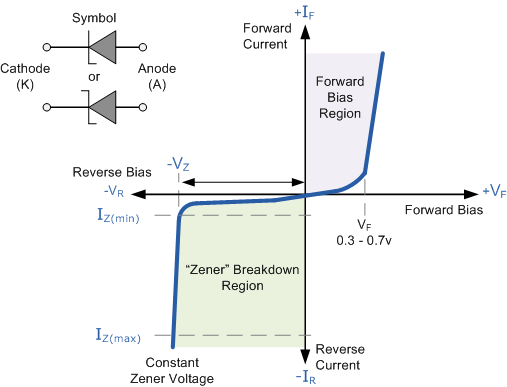
Understanding Zener Diodes and Their Core Characteristics
A zener diode functions similarly to a standard diode in forward bias but excels in reverse bias due to its controlled breakdown voltage. Unlike regular diodes that fail under reverse voltage, zener diodes are engineered to operate safely in this region, providing a stable reference voltage. Key zener diode characteristics include the zener voltage (Vz), which defines the breakdown point, typically ranging from a few volts to hundreds. The temperature coefficient indicates how Vz varies with temperature, often negative for low-voltage zeners and positive for higher ones, influencing stability across operating ranges. Dynamic impedance measures the ac resistance at the knee of the curve, affecting noise rejection and regulation quality. Power dissipation rating limits the maximum heat the device can handle, critical for sustained operation.
These characteristics make zener diodes indispensable in voltage-sensitive applications. For instance, the dynamic impedance, denoted as Zz, determines the diode's response to small signal variations, ensuring minimal ripple in regulated outputs. Engineers must evaluate datasheets for specific tolerances, as manufacturing variations impact precision. JEDEC JESD211 provides guidelines for verifying these ratings through standardized testing methods. Selecting the right zener involves balancing Vz tolerance with thermal and impedance specs for optimal performance.
The Principles Behind Zener Diode Voltage Regulation
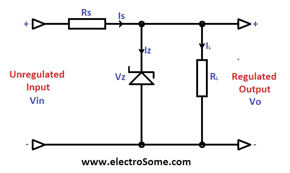
Zener diode voltage regulation relies on the shunt configuration, where the diode parallels the load across the supply. When input voltage exceeds Vz, the zener conducts, shunting excess current through a series resistor to maintain the load voltage at Vz. This self-regulating behavior stems from the sharp breakdown knee, sharper in avalanche types above 6V compared to tunneling in lower voltages. Load changes are accommodated by adjusting zener current, provided the series resistor limits total dissipation. For sensitive circuits, this technique offers simplicity over linear regulators, with lower quiescent power in light loads. However, regulation quality depends on source impedance and zener dynamic impedance.
In practice, combining multiple zeners in series can improve temperature stability and impedance. The overall voltage coefficient approaches zero near the crossover voltage around 5.6V, ideal for references. Dynamic impedance adds to the series resistor, forming an effective regulator impedance for ac signals. Engineers should simulate load steps to verify stability margins. This method shines in low-power dc supplies for op-amps or logic levels.
Zener Diode Applications in Sensitive Circuits
Zener diode applications extend beyond basic regulation to protection circuits, where they clamp transients to prevent latch-up or damage in ICs. In zener diode protection circuits, the diode is placed across inputs or power rails, activating only during overvoltages. This bidirectional clamping suits data lines, with low capacitance variants for high-speed signals. For power supplies, zeners stabilize references for feedback loops in switchers. In sensor interfaces, they reference excitation voltages precisely. Automotive and industrial boards benefit from their ruggedness under surges.
Another common use involves overvoltage crowbar circuits, tripping a fuse via zener-triggered SCR. Here, power dissipation spikes briefly, demanding robust ratings. For adc protection, select Vz just below the input's absolute maximum, paired with a current-limiting resistor. Dynamic impedance ensures fast response without ringing. These setups comply with reliability tests outlined in JEDEC standards.
Managing Zener Diode Power Dissipation and Temperature Effects
Zener diode power dissipation, calculated as P = Vz * Iz, must stay below the rated Pd, derated linearly from 25°C to maximum junction temperature. Excessive heat shifts Vz per the temperature coefficient, potentially destabilizing regulation. Low-voltage zeners exhibit negative coefficients around -2 mV/°C, while avalanche types show +2 to +5 mV/°C. Junction-to-ambient thermal resistance θja guides heatsink needs, especially on PCBs with poor copper pours. Engineers mitigate this via via stitching or thermal pads under the package.
In high-power scenarios, monitor Iz max during faults, as transients can exceed steady-state limits. Series resistors set minimum Iz for regulation and maximum for safety. PCB layout aids cooling: wide traces, ground planes, and airflow paths reduce θja. J-STD-001 soldering requirements ensure reliable thermal interfaces during assembly. Neglecting these leads to thermal runaway, where rising temperature increases Iz, accelerating failure.
Dynamic Impedance and Performance Optimization
Zener diode dynamic impedance Zzt, measured at test current Izt, quantifies small-signal regulation. Lower Zzt improves line and load rejection, akin to a resistor in parallel with the zener. At higher frequencies, capacitance shunts ac, but parasitic inductance matters in layouts. For precision, stack zeners to average coefficients and reduce effective Zz. Test under actual loads to confirm specs.
Optimization involves selecting low-Zz parts for noisy environments. Combine with capacitors for hybrid filtering. In rf circuits, minimize lead lengths to preserve impedance. These tweaks enhance overall circuit margins.
Best Practices for Implementation and Troubleshooting
When designing with zeners, start by defining rail tolerances and transient levels. Choose Vz with 5-10% margin above nominal, ensuring Iz min >5% of Iz max for knee sharpness. Calculate resistor R = (Vin max - Vz)/Iz max, verifying Pd margin. For smt packages, follow IPC J-STD-001 for void-free solder joints to maximize thermal transfer. Simulate thermal profiles and validate with scopes.
Troubleshooting begins with voltage checks: if unregulated, verify Iz range or damaged diode. Oscilloscope ripple reveals high Zz issues. Thermal camera spots hotspots. Common pitfalls include insufficient derating or poor grounding loops. Iterative testing refines designs for field reliability.
Conclusion
Zener diodes provide versatile zener diode voltage regulation for sensitive circuits, balancing simplicity with performance through tuned characteristics. Key factors like power dissipation, temperature coefficient, and dynamic impedance guide selections for protection and referencing. Adhering to best practices in design and layout ensures longevity. Engineers equipped with this knowledge can deploy zeners confidently, elevating board reliability. Future designs may integrate them with tvs for comprehensive safeguarding.
FAQs
Q1: What are the main zener diode characteristics affecting voltage regulation?
A1: Zener diode characteristics such as breakdown voltage, dynamic impedance, and temperature coefficient directly impact regulation precision. Low dynamic impedance minimizes ripple, while a stable temperature coefficient prevents drift. Power dissipation limits sustained operation under load. Select based on application needs for optimal stability in sensitive circuits.
Q2: How does zener diode power dissipation influence circuit design?
A2: Zener diode power dissipation determines safe current handling, calculated via Vz times Iz. Exceeding ratings causes thermal runaway, degrading performance. Derate for ambient temperatures and use thermal vias on PCBs. Proper series resistors prevent overloads, ensuring reliability in protection circuits.
Q3: Why consider zener diode temperature coefficient in applications?
A3: The zener diode temperature coefficient shows voltage change per degree Celsius, negative for low Vz and positive for high. Mismatch causes instability in varying environments. Zero-tc types around 5.6V suit references. Compensate with series diodes for broad temp ranges.
Q4: What role does dynamic impedance play in zener diode protection circuits?
A4: Dynamic impedance in zener diode protection circuits governs ac response, acting as parallel resistance for noise suppression. Lower values enhance transient clamping speed. Pair with capacitors for better high-frequency performance. Verify via load testing for robust safeguarding.
References
JEDEC JESD211 — Zener and Voltage Regulator Diode Reliability and Qualification Testing. JEDEC, 2009
JEDEC JESD77D — Terms, Test Methods, and Assurance Levels for Early Failure Rate Reliability of Zener Test Junction Diodes. JEDEC, 2012
IPC J-STD-001H — Requirements for Soldered Electrical and Electronic Assemblies. IPC, 2020
J-STD-020E — Moisture/Reflow Sensitivity Classification for Nonhermetic Solid State Surface Mount Devices. IPC/JEDEC, 2014


