ALLPCB


Introduction
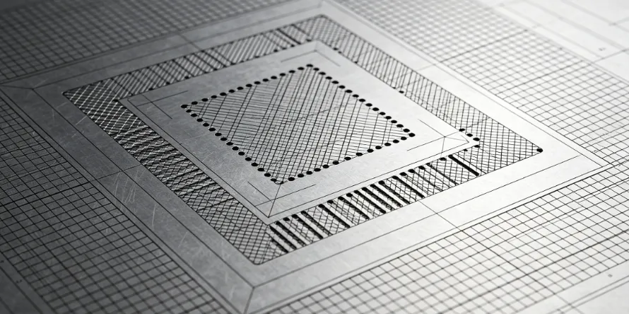
PCB stencils play a central role in surface mount technology assembly by enabling precise solder paste deposition on printed circuit boards. Once these stencils complete their service life, proper handling becomes essential to minimize environmental impact and support sustainable manufacturing practices. PCB stencil recycling addresses this need by recovering valuable materials from used stencils rather than sending them to landfills. The process aligns with broader industry efforts to reduce waste while maintaining compliance with established quality and environmental expectations. Engineers and procurement teams increasingly recognize that responsible stencil disposal contributes to both regulatory adherence and long-term operational efficiency.
Understanding PCB Stencil Recycling and Its Industry Relevance
PCB stencil recycling refers to the systematic collection, cleaning, and material recovery of stainless steel stencils after they have been used in solder paste printing operations. These stencils accumulate residues of solder paste, flux, and other contaminants during repeated use in electronics production lines. Environmentally responsible stencil disposal prevents hazardous substances from entering waste streams and allows the high-grade metal to reenter manufacturing cycles. SMT stencil recycling supports the electronics sector in meeting sustainability goals without compromising assembly quality or throughput. Recycling SMT stencils also reduces the demand for virgin raw materials, which carries both economic and ecological advantages for manufacturers.
Technical Principles Behind Stencil Material Recovery
Stencils used in PCB assembly are typically fabricated from thin stainless steel sheets that provide durability and precision during paste printing. Over time, the accumulation of solder paste and flux residues alters the stencil surface and can affect future print quality if not addressed. The recycling process begins with careful separation of organic contaminants from the metal substrate through specialized cleaning methods that preserve the integrity of the steel. Once cleaned, the stainless steel can be melted and reformed into new sheets or components suitable for additional industrial applications. This material recovery follows principles outlined in relevant IPC guidelines for handling assembly consumables, ensuring that recovered materials meet consistent performance criteria. Proper separation techniques also prevent cross-contamination that could otherwise reduce the value of the recycled output.
Best Practices for Environmentally Responsible Stencil Disposal
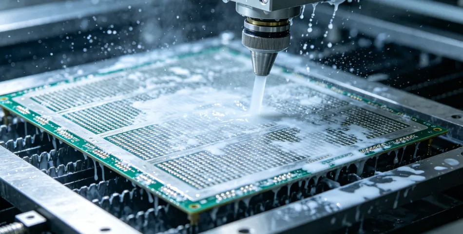
Facilities handling stencil disposal should establish clear segregation protocols that isolate used stencils from other production waste at the point of removal from the printer. Documenting the condition and quantity of each stencil supports traceability and helps recyclers optimize their processing methods. Personnel responsible for stencil management benefit from training that emphasizes safe handling of residual paste to avoid skin contact or inhalation risks during collection. Regular audits of disposal procedures help identify opportunities to increase recycling rates while maintaining alignment with ISO 14001 environmental management expectations. Collaboration with certified recycling partners ensures that recovered materials undergo appropriate downstream processing without introducing new environmental liabilities.
Practical Considerations in the Recycling Process for PCB Stencils
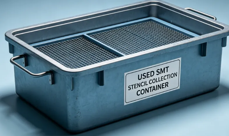
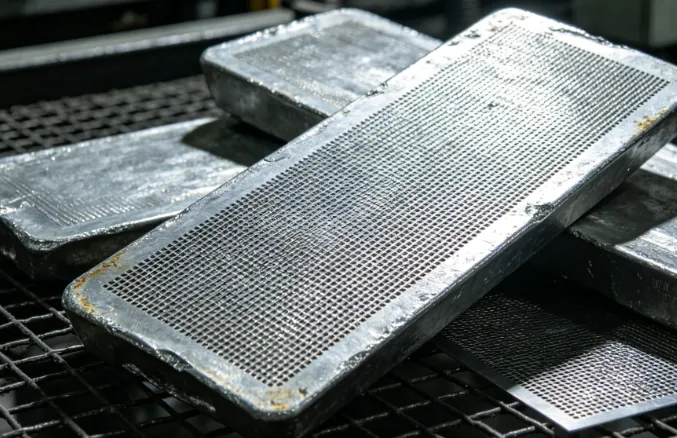
The recycling process for PCB stencils typically involves multiple stages that begin with initial inspection and end with material certification. First, stencils are transported in sealed containers to prevent residue leakage during transit. At the processing facility, mechanical and chemical cleaning steps remove solder paste and flux while capturing any valuable metals present in the residues. The cleaned stainless steel then enters a melting operation where it is refined and cast into ingots for reuse in various metal forming industries. Throughout these steps, process controls maintain consistency so that the recycled material retains the mechanical properties required for high-precision applications. Adherence to J STD 001 requirements for soldered assembly processes indirectly supports the overall integrity of material handling in electronics manufacturing environments.
Conclusion
PCB stencil recycling offers a practical pathway for electronics manufacturers to manage end-of-life stencils in an environmentally responsible manner. By focusing on material recovery and proper handling procedures, facilities can reduce waste volumes and support circular economy principles within the supply chain. Consistent application of established industry guidelines ensures that recycling efforts maintain quality and safety standards. As regulatory expectations around electronic waste continue to evolve, proactive stencil disposal practices position organizations to meet future requirements efficiently. Ultimately, integrating recycling into routine operations contributes to both environmental stewardship and operational resilience.
FAQs
Q1: What is PCB stencil recycling and why should manufacturers consider it?
A1: PCB stencil recycling involves collecting used stainless steel stencils, removing solder paste residues, and recovering the metal for reuse in other applications. This approach helps electronics manufacturers reduce landfill contributions while recovering valuable materials that would otherwise require new mining and processing. Facilities that adopt recycling programs often find improved compliance with environmental expectations and reduced long-term disposal costs. The process supports broader sustainability objectives without affecting the quality of ongoing SMT assembly operations.
Q2: How does environmentally responsible stencil disposal differ from standard waste handling?
A2: Environmentally responsible stencil disposal requires segregation of used stencils at the production line, followed by cleaning and material recovery steps that standard waste streams do not include. This method prevents solder paste residues from entering general landfills and allows the stainless steel substrate to be refined and reused. In contrast, conventional disposal may lead to higher volumes of mixed waste and lost opportunities for material reclamation. Following structured procedures also helps maintain traceability and supports alignment with recognized environmental management frameworks.
Q3: What steps are involved in the recycling process for SMT stencils?
A3: The recycling process for SMT stencils begins with safe collection and transport in sealed containers to avoid residue spillage. Cleaning operations then remove organic contaminants and solder paste, after which the stainless steel is melted and cast into new forms suitable for industrial reuse. Quality checks throughout the sequence ensure that recovered materials meet performance expectations for subsequent applications. These steps collectively minimize environmental impact while preserving the economic value of the original stencil material.
Q4: How can engineering teams ensure compliance during stencil disposal activities?
A4: Engineering teams can ensure compliance by implementing documented collection procedures and verifying that recycling partners follow established material handling protocols. Regular training for operators on residue management reduces safety risks and supports consistent process execution. Periodic reviews of disposal records help confirm that practices remain aligned with relevant industry standards for electronics manufacturing and environmental responsibility. This structured approach allows teams to integrate stencil recycling smoothly into existing quality and sustainability systems.