 ALLPCB


In high-speed printed circuit board designs, maintaining signal integrity requires careful attention to both the layer arrangement and the interconnections between those layers. Engineers must consider how signals travel through the board while minimizing reflections, crosstalk, and losses that can degrade performance. PCB stack-up defines the sequence and thicknesses of copper and dielectric layers, directly influencing impedance control and return paths. Via design, including the placement and type of vias, further determines how cleanly signals transition between layers. When these elements are optimized together, designs achieve reliable operation at multi-gigabit data rates.
What Is PCB Stack-Up and Via Design and Why It Matters
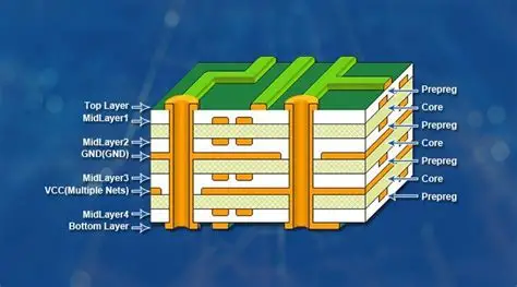
PCB stack-up refers to the planned ordering of conductive and insulating layers that form the foundation of any multilayer board. Via design encompasses the creation of plated holes that electrically connect traces on different layers, along with decisions about their size, placement, and termination. In high-speed applications, these choices become critical because even small discontinuities can introduce reflections that distort waveforms. Proper stack-up ensures consistent impedance for single-ended and differential signals, while thoughtful via implementation reduces unwanted stubs and maintains clean return paths. Without these considerations, systems operating above a few hundred megahertz often experience unacceptable bit-error rates.
Technical Principles of Signal Integrity in Stack-Up and Vias
Signal integrity depends on maintaining controlled impedance and minimizing discontinuities along the transmission path. In a multilayer board, vias act as vertical conductors that allow signals to change layers, yet they also create parasitic capacitance and inductance that alter the local impedance. When a via extends beyond the target layer, the unused portion forms a via stub that behaves like an open transmission line, causing reflections at frequencies where its length approaches a quarter wavelength. These reflections superimpose on the original signal and can close the eye diagram in high-speed serial links. Return-current paths must also remain continuous; any interruption forces the current to take a longer route, increasing loop inductance and radiated emissions.
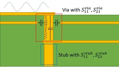
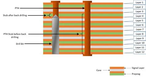
Backdrilling addresses the stub issue by removing the unused portion of the via barrel after plating. This mechanical process leaves a short, controlled via length that better matches the signal path impedance. Stack-up symmetry further supports signal integrity by balancing copper distribution, which reduces warpage during thermal cycling and keeps impedance profiles consistent across the board. Dielectric materials chosen for low loss tangent help limit attenuation at higher frequencies, while ground planes placed adjacent to signal layers provide the necessary reference for return currents. Industry standards such as IPC-6012E guide the qualification of these constructions to ensure mechanical and electrical reliability.
Related Reading: Understanding Vias in Multi-Layer PCBs: Connecting Your Circuits
Best Practices for PCB Vias and High-Speed Design
Designers begin by selecting via types that match the required layer transitions. Through-hole vias suit simple connections but introduce longer stubs unless backdrilling is applied. Blind and buried vias limit the via depth to only the necessary layers, inherently reducing stub length and improving signal integrity in dense layouts. When through-hole vias are unavoidable, specifying backdrilling with a controlled depth tolerance keeps the remaining stub short enough to push its resonant frequency above the operating bandwidth.
Stack-up planning starts with defining target impedances for all critical nets, typically 50 ohms single-ended or 100 ohms differential. Placing signal layers adjacent to solid ground planes creates microstrip or stripline configurations that deliver predictable impedance. Power planes should be positioned to supply low-inductance paths while avoiding splits directly beneath high-speed traces. Via pad and anti-pad dimensions are optimized through simulation to minimize capacitance, and stitching vias are added around connectors and component pins to maintain continuous return paths.
Related Reading: Via Design in High Frequency PCBs: Minimizing Inductance and Signal Degradation
During layout, via placement avoids clustering that could increase crosstalk, and differential pairs maintain tight coupling with matched via transitions. Simulation tools verify that the chosen stack-up and via parameters keep insertion loss and return loss within acceptable limits across the frequency range of interest. These steps collectively reduce the need for later redesigns and support first-pass success in high-speed designs.
Practical Considerations for Implementation
Engineers verify stack-up and via designs through test coupons that measure actual impedance and via performance on the manufactured board. These measurements confirm that the fabricated article matches the modeled behavior before volume production begins. Thermal and mechanical stresses during assembly can affect via integrity, so designs incorporate appropriate annular ring sizes and copper weights to withstand soldering temperatures. Documentation of all stack-up parameters and via specifications ensures consistent results across multiple fabrication lots.
Conclusion
Effective PCB stack-up and via design form the foundation for reliable signal integrity in high-speed systems. By understanding the mechanisms of reflections and impedance discontinuities, engineers can apply targeted solutions such as backdrilling and optimized layer arrangements. Consistent application of these practices, guided by established industry standards, leads to boards that perform as intended from the first prototype onward.
FAQs
Q1: How do via stubs affect signal integrity in high-speed designs?
A1: Via stubs create open-ended transmission-line segments that reflect portions of the signal energy back into the main path. At frequencies where the stub length approaches a quarter wavelength, these reflections become pronounced and degrade eye opening. Minimizing or eliminating stubs through backdrilling or blind-via usage preserves signal quality and supports higher data rates.
Q2: What role does PCB stack-up play in controlling impedance for differential pairs?
A2: PCB stack-up determines the spacing between signal layers and reference planes, which directly sets the characteristic impedance of traces and vias. Symmetric arrangements and adjacent ground planes produce predictable impedance values that remain stable across temperature and frequency variations. Proper stack-up planning therefore ensures consistent differential-pair performance throughout the board.
Q3: When should backdrilling be considered in via design?
A3: Backdrilling becomes necessary whenever through-hole vias must span multiple layers yet the signal only requires a short segment. The process removes the unused barrel length, shifting the resonant frequency of any remaining stub well above the operating bandwidth. This technique is especially valuable in designs operating above 5 Gbps where even short stubs can introduce measurable degradation.
Q4: How do industry standards influence via and stack-up decisions?
A4: Standards such as IPC-A-600K establish acceptance criteria for via fill, annular ring, and layer registration that directly impact electrical performance. Following these guidelines ensures that fabricated boards meet the mechanical and electrical requirements needed for reliable high-speed operation. Designers reference these documents early in the layout phase to align manufacturing capabilities with signal-integrity targets.
References
IPC-6012E — Qualification and Performance Specification for Rigid Printed Boards. IPC, 2017
IPC-A-600K — Acceptability of Printed Boards. IPC, 2020
JEDEC J-STD-020E — Moisture/Reflow Sensitivity Classification. JEDEC, 2014


