 ALLPCB


Introduction
PCB rework involves modifying or repairing assembled boards after initial production, and it demands careful attention to safety to avoid damage to components or injury to technicians. Engineers often perform tasks such as component replacement, solder joint repair, or trace correction, which expose them to electrical, thermal, and chemical hazards. Proper safety measures reduce the risk of electrostatic discharge that can destroy sensitive semiconductors and limit exposure to soldering fumes that irritate the respiratory system. Following established handling procedures also prevents accidental shorts that could render an entire board unusable. These practices protect both personnel and expensive test equipment during troubleshooting sessions.
Why PCB Rework Safety Matters
Rework operations occur frequently in prototype development and field repairs, where boards may already contain high-density components vulnerable to mishandling. Without adequate precautions, electrostatic discharge can cause latent failures that appear only after the board enters service. Fumes generated during desoldering release flux vapors and metal particulates that accumulate in poorly ventilated workspaces and lead to long-term health concerns. Physical contact with sharp edges or hot tools during component removal increases the chance of cuts or burns. Equipment such as oscilloscopes and power supplies can suffer from short circuits if conductive debris falls across terminals. Consistent safety routines therefore support reliable outcomes in both laboratory and production environments.
Technical Principles Behind Common Hazards
Electrostatic discharge arises when a charged body contacts a grounded conductor, transferring energy that exceeds the breakdown voltage of thin gate oxides in integrated circuits. Charge accumulation occurs through friction with clothing, carpet, or packaging materials, reaching potentials of several kilovolts in dry conditions. Thermal stress during rework can warp boards or delaminate copper traces if temperature gradients exceed material tolerances. Chemical exposure stems from rosin-based fluxes that volatilize at soldering temperatures and produce airborne irritants. Short circuits develop when solder bridges form between adjacent pads or when conductive tools bridge power and ground planes. These mechanisms interact, so a single lapse in protocol can trigger multiple failure modes simultaneously.
Practical Solutions and Best Practices
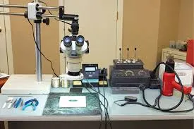
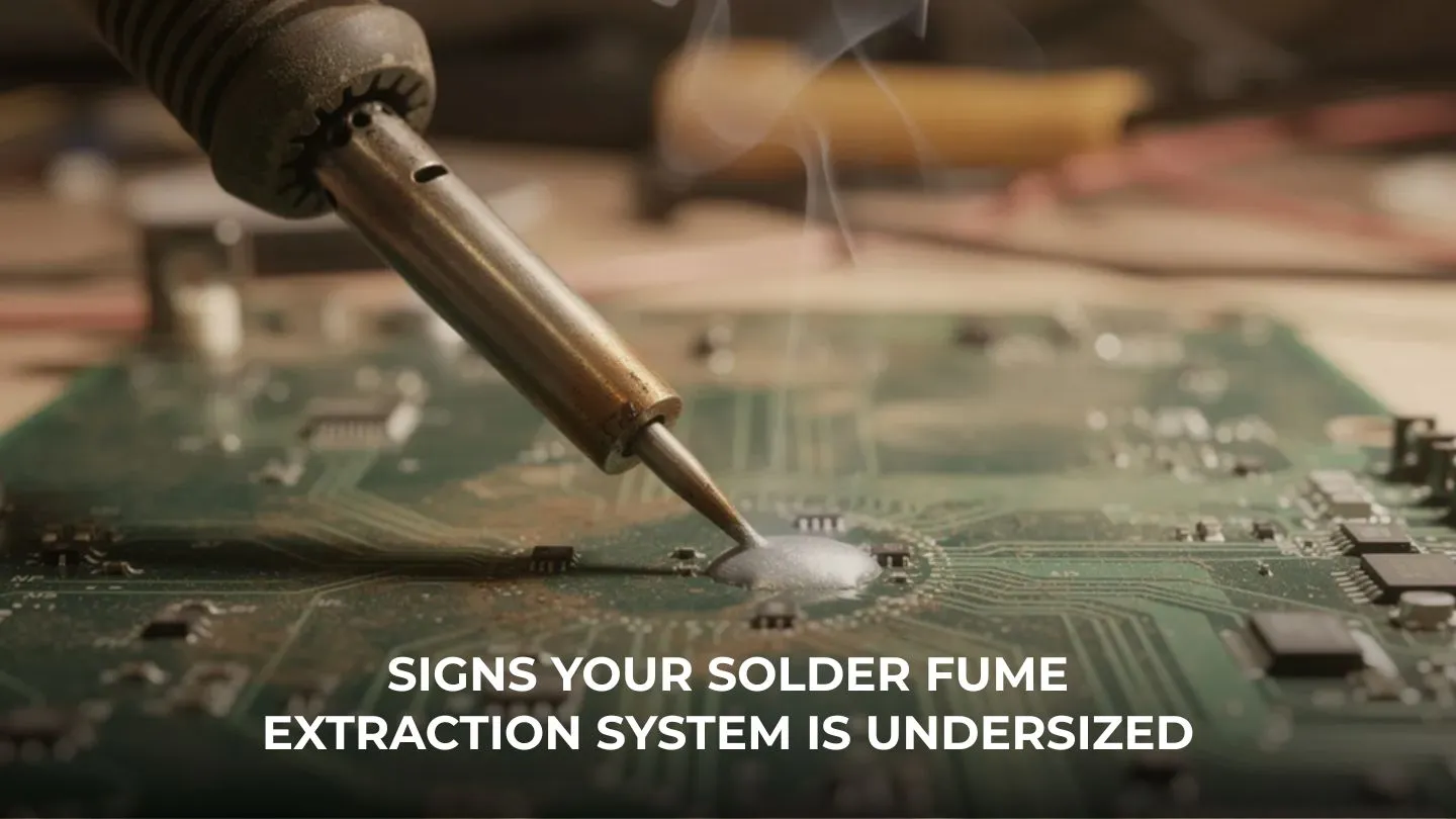
Engineers begin every rework session by grounding themselves with a wrist strap connected to a verified common point and by placing the board on a static-dissipative mat. This setup equalizes potential and channels any accumulated charge safely to earth. Fume extraction systems positioned directly above the work area capture vapors at the source and maintain air quality below occupational exposure limits. Safety glasses with side shields protect against molten solder splatter and flying debris during hot-air or iron-based removal. When handling PCBs, technicians use non-conductive tools and avoid touching component leads or exposed copper to minimize the chance of creating unintended paths. To prevent shorts, they inspect each joint under magnification after rework and apply conformal coating only after verifying isolation between traces.
Related Reading: PCB Rework: Fixing Common Assembly Errors Like a Pro
Troubleshooting Common Issues During Rework
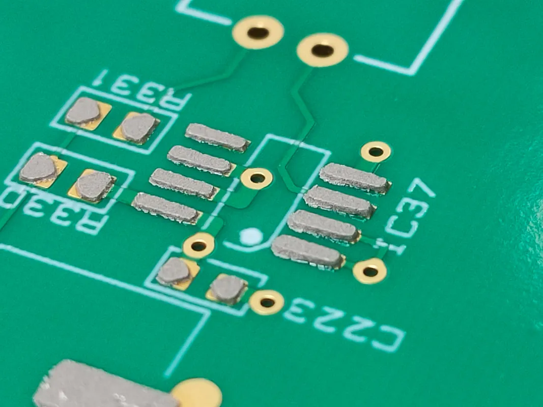
When a board exhibits unexpected behavior after component replacement, the first step is to verify that no solder bridges remain between fine-pitch leads. A continuity check with a low-voltage meter identifies these bridges before power is applied. If thermal damage appears as lifted pads or cracked traces, the rework temperature profile should be reviewed and adjusted to match the board’s thermal mass. Persistent electrostatic failures often trace back to inadequate grounding of the soldering iron tip or missing ionizer coverage over the workspace. In such cases, re-testing the entire static-control chain restores protection. These systematic checks reduce repeat failures and extend equipment life.
Related Reading: PCB Rework Station for Beginners: A Simple Guide to Component Replacement
Conclusion
Effective PCB rework safety combines electrostatic control, ventilation, personal protective equipment, and disciplined handling procedures. These measures address the primary risks of discharge, fume inhalation, and electrical shorts while preserving board integrity. Engineers who integrate these steps into daily routines achieve higher first-pass success rates and maintain compliance with recognized industry practices. Continued attention to workspace organization and tool maintenance further supports consistent, safe outcomes across repeated repair cycles.
FAQs
Q1: What steps ensure effective ESD protection during PCB rework?
A1: ESD protection begins with grounding the technician, the workbench, and all tools to a common reference point. Ionizers neutralize charges on non-conductive surfaces, while static-dissipative packaging prevents charge buildup during board transport. Regular verification of wrist-strap resistance and mat conductivity maintains the integrity of the protective chain throughout the session.
Q2: How does fume extraction improve safety in PCB rework environments?
A2: Fume extraction removes flux vapors and particulate matter directly at the soldering point, preventing their dispersion into the breathing zone. Proper placement of the nozzle and selection of appropriate filter media capture both gaseous and solid contaminants. This approach reduces respiratory irritation and supports compliance with workplace air-quality guidelines.
Q3: Why is careful handling of PCBs important for preventing shorts?
A3: Careful handling avoids contact between conductive surfaces and exposed traces or component leads. Using non-metallic tools and supporting boards only at their edges minimizes the risk of accidental bridging. Post-rework inspection confirms that no stray solder or debris remains to create low-resistance paths between power and signal lines.
Q4: What role do safety glasses play in PCB rework procedures?
A4: Safety glasses shield the eyes from molten solder droplets and flux splatter that occur during desoldering or hot-air operations. Side shields provide additional protection against particles ejected at angles. Consistent use prevents both immediate injuries and long-term vision concerns associated with repeated exposure to these hazards.





