 ALLPCB


Introduction
In the fast-evolving world of electronics, miniaturization has become a core driver for innovation across industries such as consumer devices, automotive systems, and medical equipment. PCB design engineers face constant pressure to shrink board dimensions while maintaining functionality, reliability, and manufacturability. Effective PCB layout techniques allow for significant size reductions by optimizing every aspect from component selection to routing strategies. This article explores proven engineering principles and practical methods to achieve smaller PCBs without compromising performance. By focusing on high-density interconnects and precise layout rules, designers can unlock substantial space savings. Understanding these secrets empowers electric engineers to meet demanding size constraints in modern applications.
Miniaturization not only reduces overall product footprint but also enhances portability and efficiency. PCB components play a pivotal role, as selecting the right packages directly impacts board real estate. PCB design software facilitates these optimizations, but success hinges on adherence to fundamental layout principles. Engineers must balance density with signal integrity, thermal management, and assembly feasibility. The following sections delve into the mechanisms and best practices that enable dramatic PCB size reductions.
Why Reducing PCB Size Matters
Smaller PCBs translate to compact end products, which is critical for wearables, IoT sensors, and handheld devices where space is at a premium. Miniaturization lowers material costs by using less substrate and fewer layers, while also improving power efficiency through shorter interconnects. Reduced PCB size aids thermal dissipation, as heat spreads more effectively over smaller areas with optimized copper distribution. In high-volume production, compact designs simplify enclosure integration and reduce shipping weights. Electric engineers prioritize these benefits to align with market demands for sleeker, more capable electronics.
From a performance standpoint, tighter layouts minimize parasitic inductance and capacitance, leading to better signal integrity at high frequencies. PCB components in smaller packages enable higher integration levels, supporting advanced features like 5G connectivity and AI processing. However, achieving miniaturization requires meticulous PCB design to avoid issues like crosstalk or mechanical stress. Industry trends show that boards have shrunk by orders of magnitude over decades, driven by semiconductor advances and layout innovations. Engineers who master size reduction techniques gain a competitive edge in delivering reliable, efficient solutions.
Fundamental Principles of PCB Miniaturization
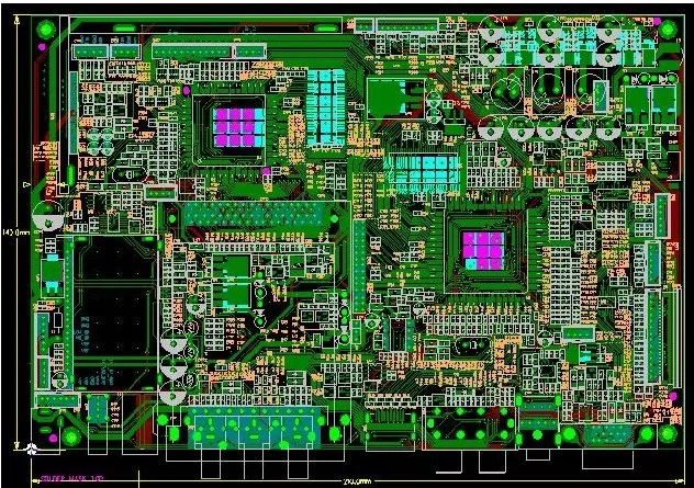
At the heart of PCB size reduction lies the principle of maximizing component density while adhering to electrical and mechanical constraints. Miniaturization begins with selecting PCB components that occupy minimal footprint, such as 0201 or smaller passives and fine-pitch BGAs. These choices allow engineers to pack more functionality into less space, but they demand precise land patterns to ensure solderability. Layout principles emphasize orthogonal placement to minimize trace lengths between interconnected elements. Signal paths must follow shortest routes to cut board area, with power and ground planes providing efficient distribution.
Another key mechanism involves trace and space scaling, where finer geometries enable routing in constrained areas. Standards like IPC-2221 outline generic rules for trace widths and clearances based on current carrying capacity and voltage levels. By tightening these dimensions within allowable limits, designers free up real estate for additional features. Vias represent a major opportunity, as traditional through-hole types consume excessive space; transitioning to smaller alternatives supports denser interconnects. Thermal considerations guide copper balancing to prevent hotspots in compact layouts. These principles form the foundation for any successful miniaturization effort.
Optimizing PCB Components for Size Reduction
Selecting the appropriate PCB components is the first step in achieving a smaller board. Engineers should prioritize surface-mount devices with the smallest available packages that meet electrical specifications, avoiding through-hole parts whenever possible. Fine-pitch components like QFNs and wafer-level packages reduce footprint while maintaining pin counts for complex circuits. Passives can shift to embedded variants within the substrate, eliminating surface area usage entirely. During schematic capture, evaluate multiple supplier datasheets to identify the most compact options without sacrificing ratings.
Land pattern design follows IPC-7351 guidelines, which specify optimal pad sizes and shapes for reliable soldering. Proper density levels, such as most dense or nominal, balance manufacturability with space savings. Component orientation plays a crucial role; aligning pins parallel to board edges shortens escape routing. Grouping analog, digital, and power sections logically minimizes cross-domain interference while packing tightly. Decoupling capacitors placed directly under ICs exemplify efficient use of under-component space. This holistic approach to PCB components ensures maximum density with minimal risk.
In practice, simulate placement early to identify conflicts. Tools allow drag-and-drop optimization, but engineering judgment refines the grid for irregular shapes. Fine-pitch BGAs require fanout strategies using dog-bone vias or direct via-in-pad for escape. By integrating these tactics, boards can shrink by integrating more per square millimeter. Reliability testing validates choices under thermal cycling and vibration.
Advanced Routing Techniques for Compact Layouts
Routing forms the backbone of PCB miniaturization, demanding precision to fit traces into tight spaces. Begin with autorouting constrained to minimum widths and spaces dictated by fabrication capabilities. Manual adjustments refine critical nets, prioritizing high-speed signals with length-matched meanders if needed. Differential pairs route as coupled lines to preserve impedance in dense areas. Power traces widen where possible, using polygons to fill unused spaces efficiently.
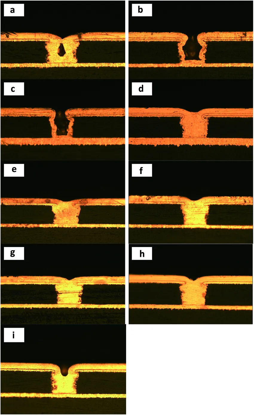
Microvias and blind vias revolutionize interconnect density, as defined in IPC-2226 for high-density interconnect boards. These features connect layers without penetrating the full stackup, saving surface routing area. Staggered or stacked microvia configurations allow any-layer interconnects in complex designs. Aspect ratios must stay conservative to ensure plating integrity, typically below 1:1. Via-in-pad techniques plug and plated-fill vias directly under components, eliminating fanout traces. This method proves essential for BGAs under 0.5mm pitch.
Bend rules minimize 90-degree corners, favoring 45-degree or curved paths to reduce reflections. Teardrops at pad junctions prevent drill breakout during fabrication. Layer pairing optimizes return paths for low inductance. Engineers iterate simulations for crosstalk and EMI, adjusting clearances accordingly. These routing secrets enable layouts that were impossible a decade ago.
Layer Stackup and Via Optimization Strategies
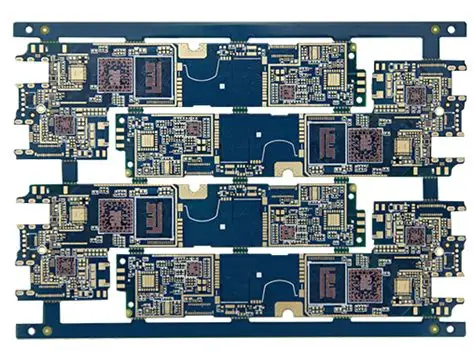
Effective layer utilization amplifies miniaturization gains. Hybrid stackups combine signal, power, and ground planes strategically to support dense routing on outer layers. Core thickness reductions enable tighter via captures, while thin dielectrics lower impedance. HDI builds add microvia layers between standard ones, classified by buildup types in relevant standards. Type III structures with multiple microvia levels achieve extreme density for processors and FPGAs.
Via optimization eliminates redundancy; share vias for multiple nets where signals permit. Filled vias in inner layers conserve space and enhance thermal conductivity. Plane splits require stitching vias around cuts to maintain continuity. Controlled impedance calculations guide dielectric choices for consistent performance. Fabricators provide DFM feedback to refine stackups pre-production.
Mechanical stability demands symmetric builds to avoid warpage. Core and prepreg balancing prevents bowing under reflow. These strategies reduce overall thickness and area simultaneously.
Best Practices and Potential Challenges
Implement design rules checks early and often to enforce miniaturization constraints. Collaborate with fabricators for capability matrices on line widths below 3 mils or microvia sizes. Partition large boards into modules if full shrinkage proves unfeasible. Prototype iterations catch routing escapes or thermal issues before full runs.
Common pitfalls include overlooking fanout for fine-pitch parts, leading to yield losses. Excessive via density risks resin voids; space them per guidelines. Signal integrity suffers from unterminated stubs in blind via transitions. Mitigate with back-drilling where applicable. Documentation of stackup and rules ensures repeatability.
Conclusion
Mastering PCB layout for size reduction demands a structured approach integrating component optimization, advanced routing, and stackup innovation. Miniaturization unlocks smaller, more efficient products while upholding reliability through standards compliance. Electric engineers applying these secrets achieve boards that pack unprecedented density. Focus on simulation, DFM, and iteration yields the best results. Future trends in substrates and vias promise even greater advances.
FAQs
Q1: How does component selection impact PCB miniaturization?
A1: Choosing smaller PCB components like 01005 resistors and fine-pitch ICs directly reduces board area in PCB design. Engineers must verify land patterns per IPC-7351 for solder joint integrity. This approach supports higher density without assembly issues. Balance size with electrical performance through derating analysis.
Q2: What role do microvias play in reducing PCB size?
A2: Microvias enable shorter interconnects in HDI structures, freeing surface space for more components. IPC-2226 provides guidelines for their implementation in PCB layout. They outperform through vias in density, ideal for BGA escape routing. Proper aspect ratios ensure reliability under thermal stress.
Q3: Can standard multilayer PCBs achieve significant miniaturization?
A3: Yes, by optimizing trace spacing and blind vias within IPC-2221 rules, standard boards shrink effectively. Focus on placement density and plane utilization for gains. Combine with fine-line etching for 20-30% area reductions in many cases. Validate with signal simulations.
Q4: What are common challenges in high-density PCB design?
A4: Density increases crosstalk and thermal risks, requiring impedance control and copper balancing. Manufacturability limits fine features, so align with fab capabilities. Troubleshooting involves DFM reviews and prototypes. Standards guide resolutions for robust outcomes.


