 ALLPCB


Introduction
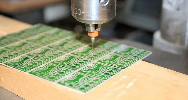
PCB drilling represents one of the most time-intensive and costly processes in printed circuit board fabrication. The operation involves creating precise vias and holes through multiple layers of substrate and copper, which demands specialized equipment and consumables. Costs escalate with factors such as hole count, diameter variations, and material properties, often accounting for a substantial share of overall manufacturing expenses. Engineers aiming for PCB drilling cost reduction must integrate design choices early, focusing on minimizing drill hole size, optimizing drill hole count, and enhancing PCB design for manufacturability. Cost-effective PCB drilling also hinges on PCB material selection for drilling, where compatibility with standard processes minimizes defects and tool wear. This article provides structured guidance for electrical engineers to implement these strategies effectively.
Why PCB Drilling Costs Matter in Manufacturing
Drilling costs arise primarily from machine runtime, drill bit consumption, and potential scrap due to misalignment or breakage. Smaller holes require finer tools that wear faster and necessitate frequent changes, amplifying expenses per board. High hole counts compound this issue, as each penetration cycle adds to processing time across panels. In high-volume production, these factors can dominate the bill of materials, making PCB drilling cost reduction essential for competitive pricing. Moreover, poor drilling quality leads to downstream issues like plating voids or reliability failures, increasing rework costs. For electrical engineers, understanding these dynamics ensures designs align with economic realities without compromising functionality.
Adhering to industry standards such as IPC-2221 for design guidelines helps mitigate risks by promoting feasible hole geometries. This standard outlines parameters that balance electrical performance with fabrication viability, indirectly supporting cost control.
Key Technical Principles of PCB Drilling Costs
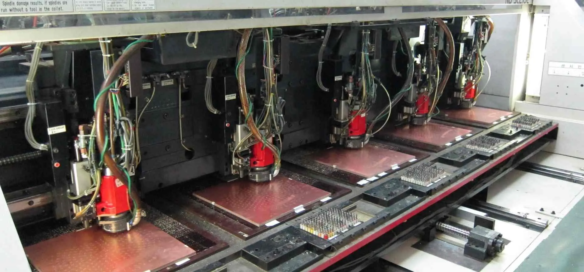
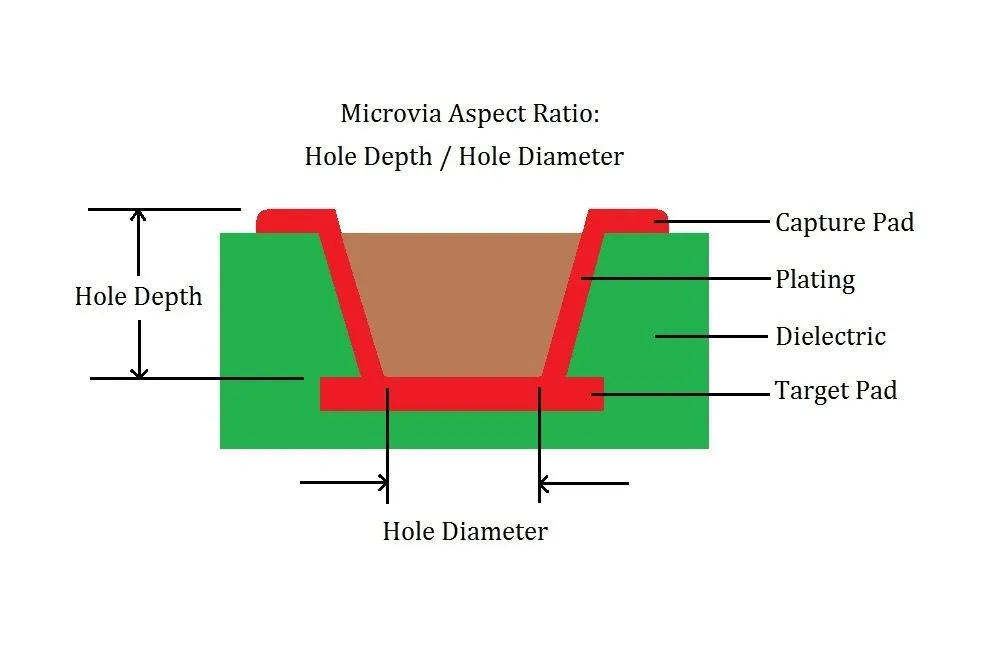
The core mechanism of PCB drilling involves high-speed carbide bits rotating at thousands of RPM to remove material layer by layer. Cost drivers include the aspect ratio, defined as board thickness divided by hole diameter, which affects chip evacuation and heat buildup. Excessive ratios lead to tapered holes, burrs, or bit breakage, requiring slower speeds or multiple passes that inflate cycle times. Material drillability varies; epoxy-based laminates generate more heat and abrasion than others, accelerating tool dulling. Hole size distribution matters too, as non-standard diameters demand unique bits, raising setup and inventory costs.
Drill hit count per panel directly correlates with total machine hours, since entry and exit marks limit panel yield. Optimizing this reduces effective cost per board. Standards like IPC-6012 provide qualification criteria for hole quality, ensuring designs stay within manufacturable limits to avoid premium pricing.
Design Tips for PCB Drilling Cost Reduction
Start with minimizing drill hole size only to the extent required for electrical needs, as excessively small vias increase costs due to precision tooling. Use the largest feasible diameter for power and ground vias to leverage standard bits, which are cheaper and longer-lasting. Group similar net connections to share vias, thereby optimizing drill hole count and reducing total penetrations. Implement blind or buried vias strategically to eliminate unnecessary through-holes that span the full stack, preserving layer integrity while cutting drilling volume.
PCB design for manufacturability emphasizes standard drill grids, typically on 2.54 mm or finer pitches aligned with component leads. Avoid arbitrary positioning that fragments drill sequences, as grouped holes allow efficient tool paths and fewer changes. Simulate routing early to consolidate vias, potentially halving hole counts in dense layouts. These practices not only lower PCB drilling cost reduction but enhance yield.
Consider fanout patterns for BGA components; standard escape routing minimizes extra vias compared to custom staggered arrays. Teardrop pads on vias distribute stress, reducing drill breakout risks during fabrication.
PCB Material Selection for Drilling Efficiency
PCB material selection for drilling profoundly impacts cost, as resin content and glass fiber weave influence cuttability. Standard FR-4 grades offer balanced drillability with moderate abrasion, making them cost-effective for most applications. Higher glass transition temperature materials resist heat better but drill harder, demanding slower feeds that extend cycle times. Select laminates with uniform resin distribution to prevent bit wandering or delamination during penetration.
Thinner cores and prepregs reduce aspect ratios inherently, easing drilling across multilayers. Verify material datasheets for drill parameters like recommended speeds and feeds to align with fab capabilities. This proactive choice supports cost-effective PCB drilling by minimizing tool wear and defect rates.
Avoid exotic reinforcements unless signal integrity demands them, as they often require specialized bits. Standard thicknesses, per IPC guidelines, further streamline processes.
Manufacturing Optimization Techniques
Panelization maximizes throughput by arraying multiple boards, spreading setup and drill change costs. Optimal array configurations consider rail spacing and fiducials for registration accuracy. Sequence drills from largest to smallest diameters to preserve bit life, as coarse tools handle roughing before fine ones finish.
Implement peck drilling for deep stacks, retracting periodically to clear chips and cool the zone. This technique, though slower, prevents hole quality issues that cause scrap. Tool management systems track usage, scheduling changes proactively to avoid mid-panel failures.
Advanced entry materials and backups stabilize the stack, reducing burrs and extending bit runs. These optimizations complement design efforts for holistic PCB drilling cost reduction.
Best Practices and Real-World Insights
In practice, reviewing Gerber files against DfM checklists catches over-specified holes early. Collaborate with fabricators on stackup proposals to favor low-aspect configurations. Track metrics like hits per bit life across prototypes to refine future designs.
For high-density interconnects, hybrid via strategies blend mechanical and laser drilling, reserving mechanical for larger holes. This divides workload efficiently, leveraging each method's strengths.
Conclusion
Effective PCB drilling cost reduction demands integrated design and manufacturing strategies. By minimizing drill hole size judiciously, optimizing drill hole count through smart routing, and prioritizing PCB design for manufacturability, engineers achieve significant savings. PCB material selection for drilling further enhances efficiency, while standards like IPC-2221 and IPC-6012 guide reliable implementation. Adopt these tips to lower costs without sacrificing performance, ensuring economical production scales.
FAQs
Q1: How can minimizing drill hole size contribute to PCB drilling cost reduction?
A1: Minimizing drill hole size requires careful electrical analysis to use only necessary diameters, avoiding premium micro-drills. Larger standard sizes reduce tool wear and change frequency, cutting cycle times. However, balance with aspect ratio limits to prevent defects. This approach, aligned with DfM principles, often yields 20-30% savings in drilling expenses for standard boards.
Q2: What role does optimizing drill hole count play in cost-effective PCB drilling?
A2: Optimizing drill hole count involves consolidating vias via net optimization and blind/buried types, reducing total penetrations per panel. Fewer holes mean shorter machine runtime and less consumable use. Design tools help simulate layouts for minimal vias while maintaining connectivity. This strategy directly lowers PCB drilling costs, especially in multilayer boards.
Q3: Why is PCB design for manufacturability key to PCB drilling cost reduction?
A3: PCB design for manufacturability incorporates standard grids, grouped holes, and feasible aspect ratios from the outset. It avoids custom tooling and fragmented sequences that inflate costs. Early DfM review ensures alignment with fab capabilities, minimizing rework. Engineers benefit from predictable pricing and higher yields.
Q4: How does PCB material selection for drilling affect overall costs?
A4: PCB material selection for drilling favors drill-friendly resins like standard FR-4 to reduce abrasion and heat. Softer composites extend bit life and allow higher speeds. Matching material to stackup lowers aspect ratios, simplifying the process. This choice integrates with design for comprehensive cost savings.
References
IPC-2221B — Generic Standard on Printed Board Design. IPC, 2012
IPC-6012E — Qualification and Performance Specification for Rigid Printed Boards. IPC, 2017
IPC-A-600K — Acceptability of Printed Boards. IPC, 2020


