 ALLPCB


Introduction
The PCB aspect ratio plays a pivotal role in determining the feasibility and economics of printed circuit board production. Defined as the ratio of the board's total thickness to the diameter of the smallest drilled hole, typically a via, this parameter directly impacts key manufacturing steps like drilling and plating. Engineers often face the challenge of achieving dense interconnects in thicker multilayer boards, which naturally increases the aspect ratio and elevates manufacturing costs through higher defect risks and rework needs. By understanding and optimizing this ratio, design teams can achieve cost efficiency without compromising electrical performance or mechanical reliability. This article delves into the technical principles, practical strategies, and factory insights for balancing PCB aspect ratio cost with production demands. Factory-driven approaches aligned with industry standards ensure defect minimization and streamlined plating processes.
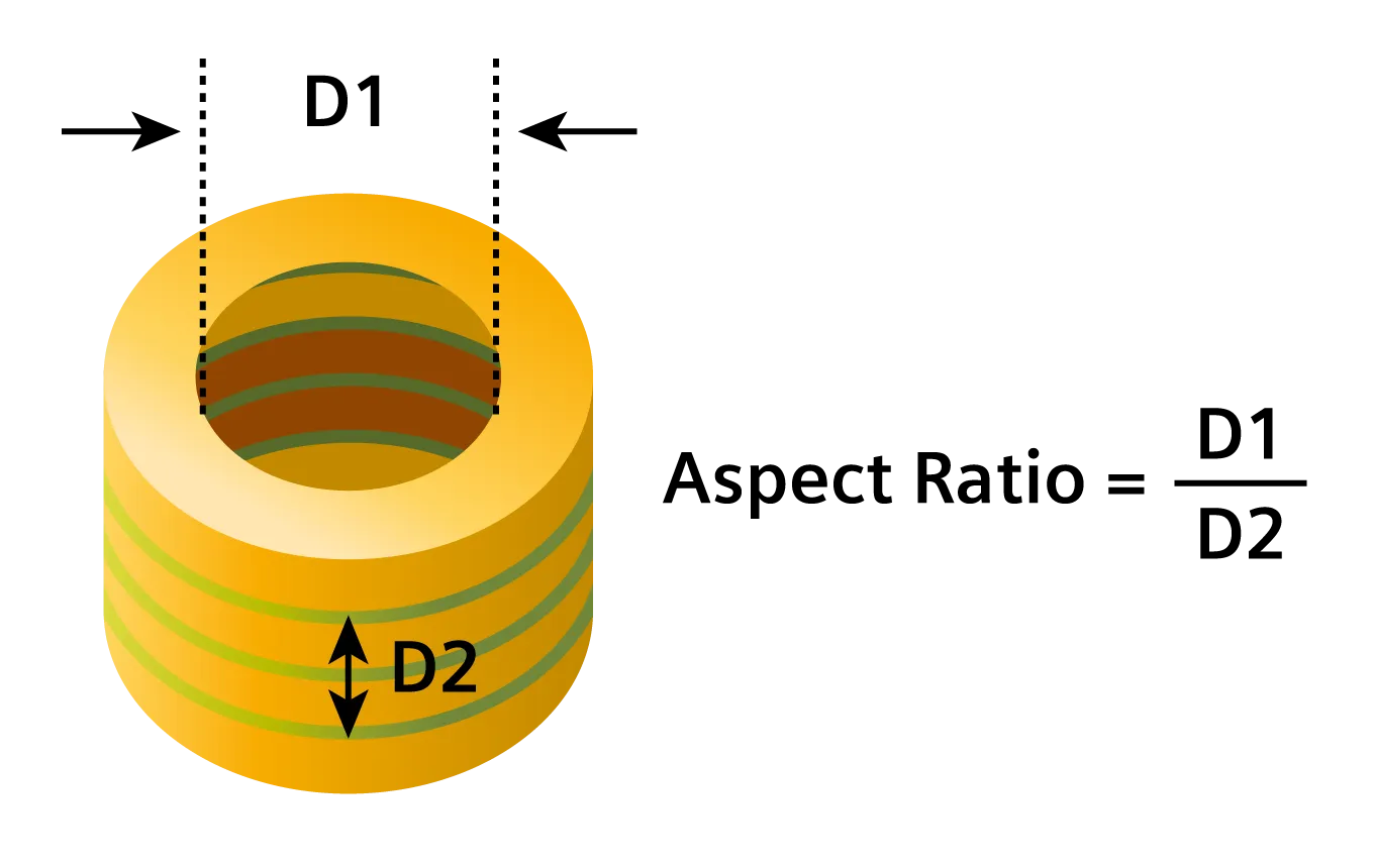
What Is PCB Aspect Ratio and Why It Matters
PCB aspect ratio is calculated by dividing the finished board thickness by the drill diameter of the smallest plated through-hole. This metric is critical because it governs the physical challenges in fabrication, particularly for vias that interconnect layers. In standard multilayer designs, board thicknesses range from 1.6 mm upward, while drill diameters shrink to accommodate high-density routing, pushing aspect ratios higher. A higher ratio complicates uniform copper deposition during the plating process, leading to potential voids or thin spots that degrade signal integrity and thermal management. From a manufacturing cost perspective, exceeding optimal ratios correlates with increased scrap rates, extended cycle times, and more frequent rework, directly inflating PCB aspect ratio cost. Prioritizing a manageable aspect ratio early in design supports cost efficiency and aligns with qualification standards like IPC-6012, which emphasize performance verification under real-world stresses.
Maintaining a balanced aspect ratio also influences overall yield in high-volume production. Factories observe that boards with ratios beyond typical limits require specialized equipment or processes, such as enhanced agitation in plating baths, adding to overhead. This not only affects unit manufacturing cost but also delays turnaround times for prototypes and production runs. Engineers must weigh these factors against performance needs, like minimizing inductance in power vias or ensuring robust mechanical strength. Ultimately, aspect ratio optimization serves as a cornerstone for defect minimization, enabling reliable boards at lower costs.
Technical Principles: How Aspect Ratio Influences Key Manufacturing Processes
Drilling Challenges with Varying Aspect Ratios
Drilling forms the foundation for via formation, and aspect ratio dictates the precision required. Higher ratios demand slower spindle speeds and specialized bits to prevent wander, breakage, or excessive taper, which can misalign layers in multilayers. The deeper the hole relative to its diameter, the greater the chip evacuation issues, risking smear or burrs that compromise plating adhesion. Factories mitigate this through peck drilling cycles, but prolonged processes raise manufacturing costs. Poor drilling quality at high aspect ratios amplifies downstream defects, necessitating additional deburring or etching steps. Consistent drill sizing matched to board thickness keeps these issues in check for cost-effective flows.
The Plating Process and Aspect Ratio Dynamics
The plating process, encompassing electroless and electrolytic copper deposition, is most sensitive to aspect ratio. In electroless plating, solutions must penetrate deep, narrow holes uniformly; high ratios reduce throwing power, resulting in thinner copper at hole bottoms and potential voids. Electrolytic plating exacerbates this if current distribution is uneven, leading to overplating on surfaces and underplating inside. IPC-2221 highlights that low aspect ratios ensure sufficient plating thickness for reliability, avoiding issues like barrel cracking under thermal cycling. Factories track copper thickness via cross-section analysis, where high-ratio boards often fail minimum specs, triggering rework. This step alone can account for significant portions of manufacturing cost when defect minimization falters.
Aspect ratio also interacts with panel processing, as grouped holes in arrays amplify inconsistencies. Advanced convection or pulse plating helps high-ratio boards, but at premium costs. Cleanliness post-desmear becomes crucial, as residues trap in deep holes, promoting defects. Optimizing ratio reduces reliance on these extras, streamlining the plating process for efficiency.
Defect Risks and Rework Implications
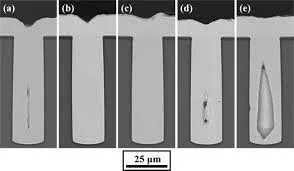
High aspect ratios elevate defect risks, including plating voids, delamination, and via opens, observed in cross-sections of failed boards. These stem from incomplete wetting during plating or mechanical stresses during lamination. IPC-A-600 provides acceptability criteria for such features, guiding visual and microscopic inspections. Rework involves stripping and replating affected panels, a labor-intensive process that delays production and hikes costs. Factories prioritize statistical process control to catch early signs, but inherent ratio challenges persist. Balancing this with performance ensures vias handle current without excessive resistance rise.
Best Practices for Optimizing PCB Aspect Ratio
Designers can target aspect ratios under 8:1 for most applications, adjusting drill diameters upward for thicker boards. This simple shift enhances plating uniformity and cuts rework incidence. Collaborate with fabricators during DFM reviews to confirm capabilities, avoiding surprises in production. Use larger vias for non-critical signals, reserving microvias for high-density areas where their shallower depth keeps effective ratios low. Blind and buried vias further reduce overall board aspect ratio by segmenting depths, though they add layering complexity.
Layer stackup planning integrates aspect ratio with material choices for CTE matching, minimizing warpage that stresses plated walls. Simulate plating throw using software to predict coverage before fabrication. Standardize hole sizes across the design to simplify tooling and drilling setups, boosting yield. These practices drive cost efficiency by minimizing defects from the outset.
Panelization strategies complement ratio optimization; grouping similar boards maximizes material use while keeping drill runs efficient. Specify finished hole sizes accounting for plating buildup, typically 0.075 mm per side. Test coupons with representative ratios validate processes early. Factories appreciate designs that avoid extreme ratios, enabling standard lines over specialized setups.
Balancing Performance and Manufacturing Cost
Performance demands like high-speed signaling favor finer vias for lower inductance, but this clashes with cost-effective manufacturing. Thicker boards for power handling increase aspect ratio, yet splitting into thinner cores with blind vias resolves this. Signal integrity models quantify trade-offs, showing acceptable losses at moderate ratios. Cost efficiency emerges from yield improvements; a 5% defect reduction translates to substantial savings in volume runs.
Factory insights reveal that iterative DFM feedback refines designs fastest. Prioritize non-functional pads larger to ease plating demands. Hybrid approaches, blending through-hole with microvias, hit sweet spots for density and cost. Long-term, these balances yield reliable boards without premium pricing.
Conclusion
Optimizing PCB aspect ratio is essential for cost-effective manufacturing, directly tying into plating process reliability, rework reduction, and defect minimization. By targeting ratios aligned with standards like IPC-2221 and IPC-6012, engineers achieve uniform plating and high yields. Practical steps, from drill sizing to via strategies, balance dense layouts with economic fabrication. Factory-driven DFM ensures these principles translate to real production gains. Ultimately, thoughtful aspect ratio management delivers performance without excessive PCB aspect ratio cost, supporting scalable electronics development.
FAQs
Q1: What is the main impact of PCB aspect ratio on manufacturing cost?
A1: High PCB aspect ratios increase manufacturing cost primarily through challenges in the plating process and higher rework rates. Narrow, deep holes hinder uniform copper deposition, leading to voids and yield losses that require panel stripping or scrapping. Keeping ratios under standard limits, such as those in IPC guidelines, minimizes these issues and supports cost efficiency in volume production. Designers should prioritize this early to avoid premium processes.
Q2: How does aspect ratio affect the plating process in PCB fabrication?
A2: Aspect ratio governs solution penetration and throwing power during electroless and electrolytic plating. Higher ratios cause thinner plating at hole bottoms, risking defects like incomplete coverage or cracks. Factories use enhanced agitation for mitigation, but standard ratios ensure compliance with thickness requirements per IPC-6012. This directly influences plating process reliability and overall cycle time.
Q3: What best practices help with defect minimization related to PCB aspect ratio?
A3: Target aspect ratios below 8:1, use larger drills for thick boards, and incorporate blind vias to segment depths. DFM collaboration verifies fabricator capabilities, reducing plating defects and rework. Cross-section coupons confirm plating uniformity early. These steps align with IPC-A-600 acceptability, promoting defect minimization and cost efficiency.
Q4: How can engineers achieve cost efficiency while optimizing PCB aspect ratio?
A4: Balance via sizing with stackup to keep ratios manageable, simulating plating coverage beforehand. Standardize hole patterns for efficient drilling and avoid extremes requiring special equipment. Factory feedback on DFM refines designs, cutting manufacturing cost through higher yields. This approach maintains performance in high-density boards.
References
IPC-2221A — Generic Standard on Printed Board Design. IPC.
IPC-6012E — Qualification and Performance Specification for Rigid Printed Boards. IPC, 2017.
IPC-A-600K — Acceptability of Printed Boards. IPC, 2020.


