 ALLPCB


Introduction
PCB designers face critical decisions when balancing minimum line width with signal frequency requirements. High-frequency signals demand precise control over trace dimensions to maintain signal integrity and minimize losses. Factors such as PCB trace width for high frequency signals directly influence performance in applications like RF circuits and high-speed digital interfaces. Understanding the interplay between minimum line width signal loss and signal integrity trace width frequency ensures reliable operation. This guide provides logical, structured explanations for electrical engineers, drawing on established engineering principles. By optimizing these parameters, designers can achieve robust designs that meet performance targets.
Defining Minimum Line Width and Its Relevance to Signal Frequency
Minimum line width refers to the smallest allowable dimension for conductive traces on a printed circuit board, governed by manufacturing capabilities and quality standards. IPC-A-600 outlines acceptability criteria for conductor widths across different board classes, ensuring consistency in production. For high-frequency applications, this width must accommodate electrical characteristics beyond mere fabrication limits. Signal frequency dictates the need for wider traces in some cases to reduce resistance and control impedance, while narrower traces suit dense layouts but risk increased attenuation. Engineers must evaluate the frequency content of signals, often approximating the knee frequency as half the rise time inverse, to determine suitable widths. This relationship underscores why PCB trace width for high frequency signals cannot be treated in isolation from overall design goals.
Core Technical Principles: Signal Propagation and Trace Geometry
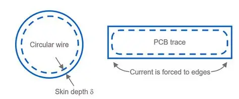
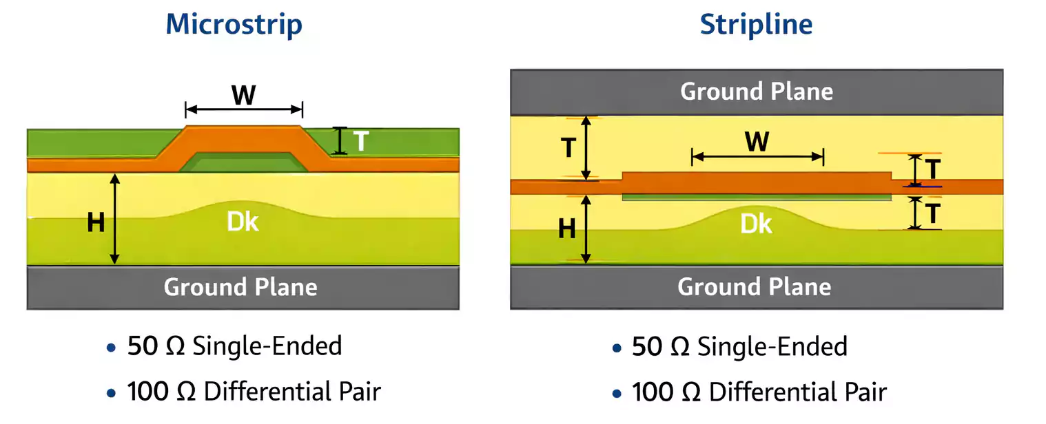
At high frequencies, skin effect confines current to the trace surface, effectively reducing cross-sectional area and elevating resistance. The skin depth decreases proportionally with the square root of frequency, making narrow traces particularly susceptible to higher losses. Conductor loss becomes dominant in minimum line width signal loss scenarios, where attenuation coefficient alpha_c scales with sqrt(f) and inversely with width. Dielectric losses also interact, as trace width influences the field distribution between conductor and substrate. Characteristic impedance Z0 for microstrip lines depends on trace width relative to dielectric height, following formulas derived from transmission line theory. Proper sizing prevents mismatches that cause reflections, degrading signal integrity trace width frequency balance.
Engineers calculate Z0 using width-to-height ratios, typically targeting 50 ohms for single-ended signals or 100 ohms for differential pairs. As frequency rises into GHz ranges, radiation losses emerge if traces lack shielding, further emphasizing width optimization. Capacitive and inductive coupling between adjacent traces scales with proximity and width, necessitating spacing rules like 3W for crosstalk mitigation. These principles form the foundation for designing traces that preserve waveform fidelity across bandwidths.
Key Factors Influencing Minimum Line Width at High Frequencies
Fabrication process defines the absolute minimum line width, often starting at 3-4 mils for standard processes and finer for HDI. Stackup configuration affects field confinement, with embedded traces allowing narrower widths due to symmetric fields. Material properties, including dielectric constant and loss tangent, interact with width to determine total insertion loss. Signal rise time and harmonic content dictate effective frequency, requiring wider traces for lower loss in broadband applications. Thermal considerations, per IPC-2221 guidelines, ensure widths support current without excessive heating, even if high-frequency signals carry low DC current. Environmental factors like humidity can exacerbate losses in narrow traces by altering dielectric performance.
Copper thickness influences skin effect penetration; thicker foils permit slightly narrower effective widths at very high frequencies. Routing length amplifies cumulative losses, pushing designers toward wider traces for long runs. Impedance tolerance, often +/-10%, demands precise width control during layout. These factors collectively guide decisions on PCB trace width for high frequency signals.
Best Practices for Trace Width Optimization in High-Frequency PCB Design
Start with impedance-controlled routing, using field solvers to compute width based on stackup and target Z0. IPC-2221 provides design aids for initial sizing, emphasizing balanced proportions for performance. Implement length-matching for differential pairs to preserve timing skew, adjusting widths uniformly. Employ ground planes adjacent to signal traces to reference fields and reduce radiation. For minimum line width signal loss concerns, simulate insertion loss versus frequency curves to validate choices. Gradually taper widths in transitions to avoid discontinuities.
Adopt conservative spacing, at least three times the trace width, to suppress near-end and far-end crosstalk. Use via fences or stitching for shielding in critical sections. Verify designs through time-domain reflectometry modeling to catch reflections early. During layout, prioritize shorter routes for highest frequencies to minimize dispersion. Post-layout extraction confirms signal integrity trace width frequency compliance before fabrication.
Troubleshooting Common Issues in High-Frequency Trace Designs
Narrow traces often exhibit excessive attenuation, manifesting as eye closure in simulations. Increase width or switch to lower-loss dielectrics while respecting space constraints. Reflections from impedance steps cause ringing; smooth transitions with polygons or arcs. Crosstalk appears as noise on victim traces; widen spacing or add guards. Fabricated boards failing electrical tests may stem from etch tolerances; reference IPC-A-600 for acceptable variations. Iterate with prototypes, measuring S-parameters to correlate models with reality.
Excessive radiation in unshielded designs leads to EMI; enclose traces in cavities or use embedded components. Thermal hotspots from power traces nearby degrade high-frequency performance; separate analog and digital sections.
Conclusion
Mastering minimum line width and signal frequency requires integrating fabrication limits with electromagnetic principles. PCB trace width for high frequency signals must prioritize low loss and controlled impedance for optimal signal integrity. By applying structured calculations and verification, engineers mitigate minimum line width signal loss effectively. Adhering to signal integrity trace width frequency guidelines ensures designs perform reliably in demanding applications. This approach yields robust PCBs ready for production.
FAQs
Q1: How does PCB trace width affect high frequency signals?
A1: PCB trace width influences characteristic impedance and conductor losses in high frequency signals. Narrower widths increase skin effect resistance, leading to higher attenuation at GHz frequencies. Designers calculate widths to match target Z0, typically using stackup-specific ratios. Wider traces reduce losses but consume more space, balancing density and performance. Simulations confirm integrity across the signal bandwidth.
Q2: What causes minimum line width signal loss in PCBs?
A2: Minimum line width signal loss arises primarily from skin effect and ohmic resistance at high frequencies. Current crowds to trace edges, reducing effective conducting area. Dielectric interactions amplify total loss for narrow geometries. IPC-2221 aids in selecting widths to minimize this. Proper sizing preserves signal amplitude over long traces.
Q3: Why is signal integrity trace width frequency critical for PCB design?
A3: Signal integrity trace width frequency is critical because higher frequencies demand precise impedance control to avoid reflections. Trace width determines Z0 and coupling, affecting waveform distortion. Bandwidth considerations guide minimum widths to curb dispersion. Electrical engineers optimize via modeling for clean eye patterns. This ensures data rates without errors.
Q4: What are best practices for minimum line width in high-speed PCBs?
A4: For high-speed PCBs, select minimum line width based on fab class per IPC-A-600, then adjust for impedance. Use 3W spacing rules to limit crosstalk. Simulate losses versus frequency for validation. Prefer symmetric stackups for consistent performance. Prototype testing refines final dimensions.
References
IPC-2221B — Generic Standard on Printed Board Design. IPC, 2009
IPC-A-600K — Acceptability of Printed Boards. IPC, 2020
IPC-2152A — Standard for Determining Current Carrying Capacity in Printed Board Design. IPC, 2009


