 ALLPCB


Why Reliability Matters in HDI PCB Design
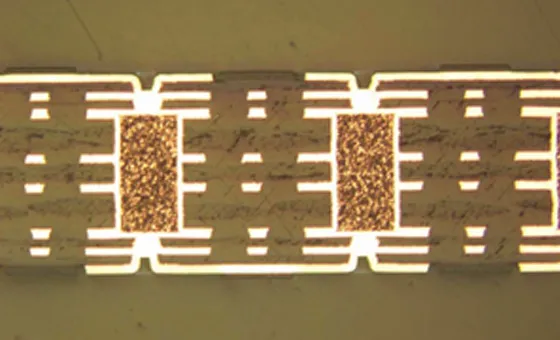
Microvias are small conductive holes, typically under 150 micrometers in diameter, that link adjacent layers in multilayer boards. In HDI PCB design they replace larger through-holes, freeing up routing space and supporting finer pitch components. Poor microvia reliability can lead to open circuits, intermittent connections, or accelerated fatigue during temperature cycling. Procurement teams and design engineers therefore evaluate microvia construction early to match the expected operating environment. Reliable microvias contribute directly to overall product lifespan and reduce field returns.
Technical Principles Behind Microvia Failures
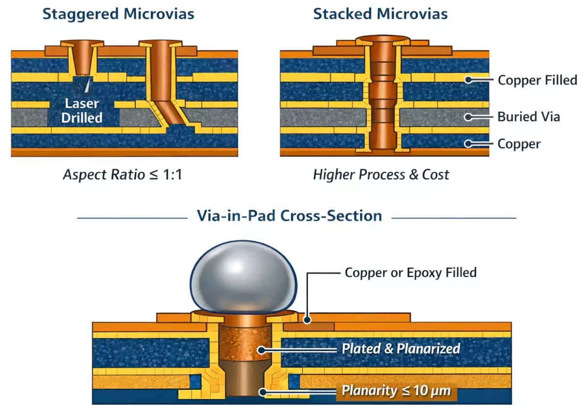
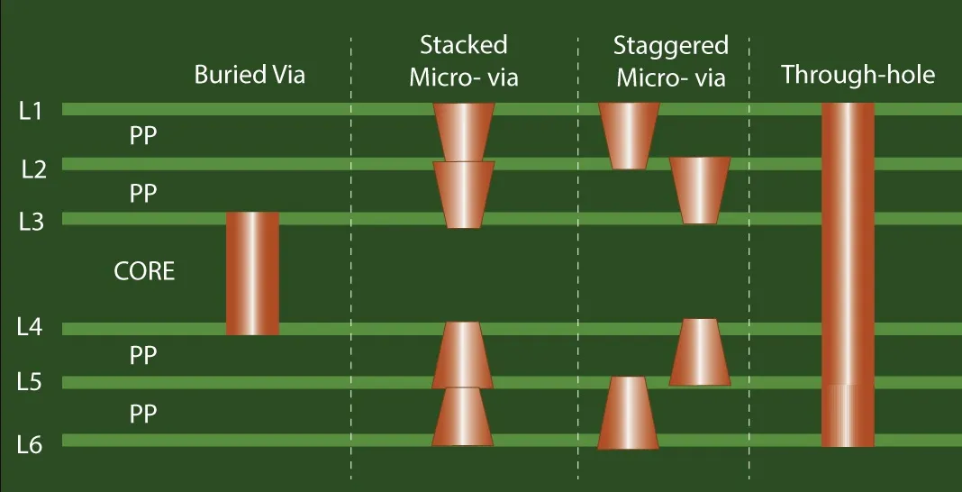
Laser drilling creates the initial hole in the dielectric material. The process must remove resin and glass fibers cleanly without excessive charring or delamination. Any residue left inside the hole can interfere with subsequent copper plating and create weak spots. Stacked vias place multiple microvias directly on top of one another to achieve higher layer counts. This configuration concentrates stress at the interfaces during thermal expansion. Staggered vias offset each connection slightly, distributing mechanical load more evenly across the build-up layers. Copper plating voids occur when electrolyte fails to reach the bottom or sidewalls of the microvia during electroplating. These voids reduce the effective cross-sectional area available for current flow and become initiation sites for cracks under repeated thermal cycling.
Related Reading: Advanced FR 4 PCB Techniques: High Density Interconnect (HDI) and Microvias
Practical Solutions and Best Practices for Improved Microvia Reliability
Design teams begin by selecting dielectric materials with coefficients of thermal expansion matched to the copper conductors. This reduces shear stress at the microvia barrel during temperature changes. Engineers also specify minimum copper thickness on the microvia walls according to the expected current density. During manufacturing, sequential build-up processes with controlled lamination pressure help maintain hole integrity before plating. Post-plating inspection using cross-sectio
n analysis verifies that voids remain below acceptable limits. Thermal cycling tests performed to relevant industry standards confirm that the chosen microvia structure will survive the intended service life. Staggered via patterns are often preferred when board thickness and layer count allow, because they lower the risk of crack propagation compared with stacked arrangements.
Related Reading: Microvia Testing: Ensuring Reliability in HDI PCBs
Troubleshooting Common Microvia Issues in Production
When electrical opens appear after reflow, the first step is to examine the plating quality inside the microvias. Incomplete copper coverage often traces back to inadequate desmear or insufficient agitation during the plating bath. If failures occur only after multiple thermal cycles, the root cause frequently lies in the via stacking strategy or the choice of build-up material. Engineers can adjust the stagger distance or introduce additional capture pads to improve mechanical compliance. In cases where laser drilling parameters produce tapered holes, modifying pulse energy and focus settings restores a more cylindrical profile that plates more uniformly. Collaboration between the design and fabrication teams at this stage prevents repeated iterations and keeps the project on schedule.
Conclusion
Microvia reliability in HDI PCB design depends on careful attention to drilling, plating, and via arrangement. Stacked and staggered configurations each carry distinct mechanical implications that must be evaluated against the product requirements. Addressing copper plating voids through process control and material selection reduces the most common failure modes. By following established industry practices, engineering teams can deliver boards that maintain electrical integrity throughout their operational life. Consistent application of these principles supports both performance goals and manufacturing yield.
FAQs
Q1: What factors most influence microvia reliability in HDI PCB design?
A1: Microvia reliability is affected by drilling quality, plating uniformity, via stacking method, and material selection. Stacked vias concentrate stress while staggered vias distribute it more evenly. Proper control of these elements during design and fabrication helps prevent opens and fatigue failures.
Q2: How does laser drilling affect copper plating voids in microvias?
A2: Laser drilling must produce clean, cylindrical holes without excessive residue. Residual material can block electrolyte flow and create voids during copper plating. Adjusting laser parameters and following desmear procedures minimizes these defects and improves long-term electrical continuity.
Q3: When should designers choose staggered vias over stacked vias?
A3: Staggered vias are preferred when thermal cycling or mechanical shock is expected, because they reduce stress concentration at any single interface. Stacked vias allow higher density but require additional design margins or reinforced plating to achieve comparable reliability.
Q4: What role do industry standards play in verifying microvia reliability?
A4: Standards such as IPC-6012E provide acceptance criteria for plated hole quality and overall board performance. Following these guidelines during qualification testing ensures that microvia structures meet the mechanical and electrical demands of the application.
References
IPC-6012E - Qualification and Performance Specification for Rigid Printed Boards. IPC, 2017
IPC-A-600K - Acceptability of Printed Boards. IPC, 2020
JEDEC J-STD-020E - Moisture/Reflow Sensitivity Classification. JEDEC, 2014


